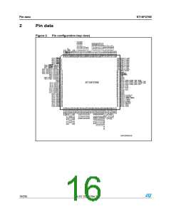
Pin data
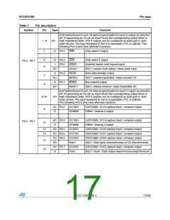
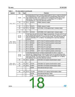
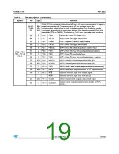
Table 1.
ST10F276E
Pin description (continued)
Symbol
Pin
Type
Function
Port 4 is an 8-bit bidirectional I/O port. It is bit-wise programmable for input or
output via direction bit. Programming an I/O pin as input forces the
corresponding output driver to high impedance state. The input threshold is
85-92
I/O selectable (TTL or CMOS). Port 4.4, 4.5, 4.6 and 4.7 outputs can be configured
as push-pull or open drain drivers.
In case of an external bus configuration, Port 4 can be used to output the
segment address lines:
85
86
87
88
89
O
O
O
O
O
I
P4.0
P4.1
P4.2
P4.3
P4.4
A16
A17
A18
A19
A20
Segment address line
Segment address line
Segment address line
Segment address line
Segment address line
CAN2_RxD CAN2: receive data input
P4.0 –P4.7
I/O
O
I
SCL
A21
I2C Interface: serial clock
90
91
92
P4.5
P4.6
P4.7
Segment address line
CAN1_RxD CAN1: receive data input
CAN2_RxD CAN2: receive data input
I
O
O
O
O
O
I/O
A22
Segment address line
CAN1_TxD CAN1: transmit data output
CAN2_TxD CAN2: transmit data output
A23
Most significant segment address line
CAN2_TxD CAN2: transmit data output
SDA
I2C Interface: serial data
External memory read strobe. RD is activated for every external instruction or
data read access.
RD
95
96
O
External memory write strobe. In WR-mode this pin is activated for every
external data write access. In WRL mode this pin is activated for low byte data
write accesses on a 16-bit bus, and for every data write access on an 8-bit bus.
See WRCFG in the SYSCON register for mode selection.
WR/WRL
O
Ready input. The active level is programmable. When the ready function is
enabled, the selected inactive level at this pin, during an external memory
access, will force the insertion of waitstate cycles until the pin returns to the
selected active level.
READY/
READY
97
98
I
Address latch enable output. In case of use of external addressing or of
multiplexed mode, this signal is the latch command of the address lines.
ALE
O
20/235
Doc ID 12303 Rev 3

 STMICROELECTRONICS [ ST ]