ST10F276E
Electrical characteristics
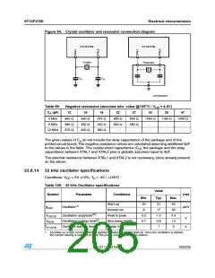
Figure 54. Crystal oscillator and resonator connection diagram
34ꢀꢉ&ꢁꢊꢄ%
#RYSTAL
34ꢀꢉ&ꢁꢊꢄ%
2ESONATOR
#
#
!
!
'!0'2)ꢉꢉꢈꢈꢃ
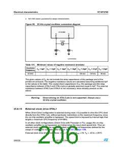
Table 99. Negative resistance (absolute min. value @125oC / VDD = 4.5V)
CA (pF)
12
15
18
22
27
33
39
47
4 MHz
8 MHz
12 MHz
460 Ω
380 Ω
370 Ω
550 Ω
460 Ω
420 Ω
675 Ω
540 Ω
360 Ω
800 Ω
640 Ω
-
840 Ω
580 Ω
-
1000 Ω
1180 Ω
1200 Ω
-
-
-
-
-
-
The given values of CA do not include the stray capacitance of the package and of the
printed circuit board: The negative resistance values are calculated assuming additional 5pF
to the values in the table. The crystal shunt capacitance (C0), the package and the stray
capacitance between XTAL1 and XTAL2 pins is globally assumed equal to 4pF.
The external resistance between XTAL1 and XTAL2 is not necessary, since already present
on the silicon.
23.8.14 32 kHz oscillator specifications
Conditions: VDD = 5V 10%, TA = -40 / +125°C
Table 100. 32 kHz Oscillator specifications
Value
Typ.
Symbol
Parameter
Conditions
Unit
Min.
Max.
Start-up
20
8
31
17
1.0
0.9
1
50
30
2.4
1.2
5
gm32
Oscillator(1)
µA/V
Normal run
VOSC32
VAV32
Oscillation amplitude(2))
Oscillation-voltage level(2)
Oscillator start-up time(2)
Peak to peak
Sine wave middle
Stable VDD
0.5
0.7
-
V
s
tSTUP32
1. At power-on a high current biasing is applied for faster oscillation start-up. Once the oscillation is started,
the current biasing is reduced to lower the power consumption of the system.
Doc ID 12303 Rev 3
205/235

 STMICROELECTRONICS [ ST ]