Electrical characteristics
ST10F276E
23.8.17 External memory bus timing
In the next sections the external memory bus timings are described. The given values are
computed for a maximum CPU clock of 40 MHz.
It is evident that when higher CPU clock frequency is used (up to 64 MHz), some numbers in
the timing formulas become zero or negative, which in most cases is not acceptable or
meaningful. In these cases, the speed of the bus settings tA, tC and tF must be correctly
adjusted.
Note:
All external memory bus timings and SSC timings presented in the following tables are given
by design characterization and not fully tested in production.
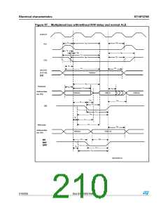
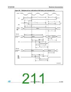
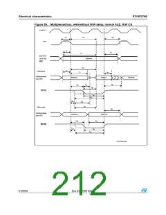
23.8.18 Multiplexed bus
VDD = 5V 10%, VSS = 0V, TA = -40 to +125°C, CL = 50pF,
ALE cycle time = 6 TCL + 2tA + tC + tF (75ns at 40 MHz CPU clock without wait states).
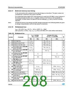
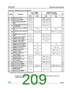
Table 104. Multiplexed bus
f
CPU = 40 MHz
Variable CPU clock
TCL = 12.5ns
1/2 TCL = 1 to 64 MHz
Symbol
Parameter
Min.
Max.
Min.
Max.
t5
t6
t7
CC ALE high time
4 + tA
1.5 + tA
4 + tA
TCL - 8.5 + tA
TCL - 11 + tA
TCL - 8.5 + tA
ns
ns
ns
CC Address setup to ALE
CC Address hold after ALE
-
-
ALE falling edge to RD, WR
(with RW-delay)
t8
t9
CC
4 + tA
TCL - 8.5 + tA
- 8.5 + tA
ns
ns
ns
ns
ns
ns
ns
ns
ALE falling edge to RD, WR
(no RW-delay)
CC
- 8.5 + tA
Address float after RD, WR
t10 CC
t11 CC
t12 CC
t13 CC
t14 SR
t15 SR
6
6
(with RW-delay)(1)
-
-
Address float after RD, WR
(no RW-delay)(1)
18.5
TCL + 6
RD, WR low time
(with RW-delay)
15.5 + tC
28 + tC
2TCL - 9.5 + tC
3TCL - 9.5 + tC
-
-
RD, WR low time
(no RW-delay)
RD to valid data in
(with RW-delay)
6 + tC
2TCL - 19 + tC
3TCL - 19 + tC
RD to valid data in
(no RW-delay)
18.5 + tC
-
-
t16 SR ALE low to valid data in
17.5 + tA + tC
20 + 2tA + tC
3TCL - 20 + tA + tC ns
4TCL - 30 + 2tA + tC ns
Address/Unlatched CS to
t17 SR
valid data in
Data hold after RD
t18 SR
0
-
-
0
-
-
ns
ns
rising edge
t19 SR Data float after RD
16.5 + tF
2TCL - 8.5 + tF
208/235
Doc ID 12303 Rev 3

 STMICROELECTRONICS [ ST ]