ST10F276E
Electrical characteristics
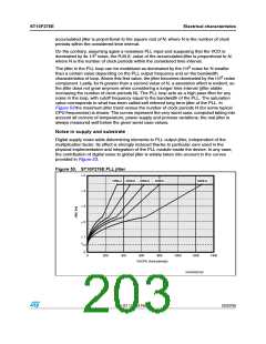
accumulated jitter is proportional to the square root of N, where N is the number of clock
periods within the considered time interval.
On the contrary, assuming again a noiseless PLL input and supposing that the VCO is
dominated by its 1/f3 noise, the R.M.S. value of the accumulated jitter is proportional to N,
where N is the number of clock periods within the considered time interval.
The jitter in the PLL loop can be modelized as dominated by the i1/f2 noise for N smaller
than a certain value depending on the PLL output frequency and on the bandwidth
characteristics of loop. Above this first value, the jitter becomes dominated by the i1/f3 noise
component. Lastly, for N greater than a second value of N, a saturation effect is evident, so
the jitter does not grow anymore when considering a longer time interval (jitter stable
increasing the number of clock periods N). The PLL loop acts as a high pass filter for any
noise in the loop, with cutoff frequency equal to the bandwidth of the PLL. The saturation
value corresponds to what has been called self referred long term jitter of the PLL. In
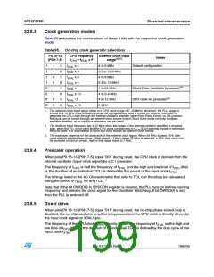
Figure 53 the maximum jitter trend versus the number of clock periods N (for some typical
CPU frequencies) is shown: The curves represent the very worst case, computed taking into
account all corners of temperature, power supply and process variations; the real jitter is
always measured well below the given worst case values.
Noise in supply and substrate
Digital supply noise adds determining elements to PLL output jitter, independent of the
multiplication factor. Its effect is strongly reduced thanks to particular care used in the
physical implementation and integration of the PLL module inside the device. In any case,
the contribution of digital noise to global jitter is widely taken into account in the curves
provided in Figure 53.
Figure 53. ST10F276E PLL jitter
rꢀꢃ
ꢀꢄ-(Z ꢁꢇ-(Z ꢈꢁ-(Z
ꢇꢉ-(Z
ꢄꢇ-(Z
rꢀꢇ
rꢀꢈ
rꢀꢁ
rꢀꢀ
4
*)4
ꢉ
ꢉ
ꢁꢉꢉ
ꢇꢉꢉ
ꢄꢉꢉ
ꢆꢉꢉ
ꢀꢉꢉꢉ
ꢀꢁꢉꢉ
ꢀꢇꢉꢉ
. ꢍ#05 CLOCK PERIODSꢏ
'!0'2)ꢉꢉꢀꢈꢉ
Doc ID 12303 Rev 3
203/235

 STMICROELECTRONICS [ ST ]