ST10F276E
Electrical characteristics
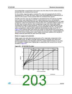
PLL usage
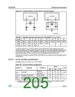
Table 102. External clock drive timing
Direct drive with
prescaler
fCPU = fXTAL / 2
Direct drive
fCPU = fXTAL
fCPU = fXTAL x F
Symbol
Parameter
Unit
Min.
OSCSR XTAL1 period(1) (2) 15.625
Max.
Min.
Max.
Min.
Max.
t
-
83.3
250
83.3
250
t1 SR High time(3)
t2 SR Low time(3)
t3 SR Rise time(3)
t4 SR Fall time(3)
6
-
-
3
-
-
6
-
-
ns
2
2
2
1. The minimum value for the XTAL1 signal period is considered as the theoretical minimum. The real
minimum value depends on the duty cycle of the input clock signal.
2. 4-12 MHz is the input frequency range when using an external clock source. 64 MHz can be applied with
an external clock source only when Direct Drive mode is selected: In this case, the oscillator amplifier is
bypassed so it does not limit the input frequency.
3. The input clock signal must reach the defined levels V and V
.
IL2
IH2
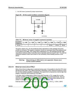
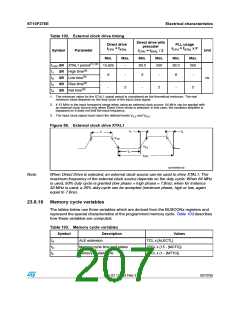
Figure 56. External clock drive XTAL1
T
T
T
ꢈ
ꢇ
ꢀ
6
)(ꢁ
6
),ꢁ
T
ꢁ
T
/3#
'!0'2)ꢉꢉꢀꢈꢈ
Note:
When Direct Drive is selected, an external clock source can be used to drive XTAL1. The
maximum frequency of the external clock source depends on the duty cycle: When 64 MHz
is used, 50% duty cycle is granted (low phase = high phase = 7.8ns); when for instance
32 MHz is used, a 25% duty cycle can be accepted (minimum phase, high or low, again
equal to 7.8ns).
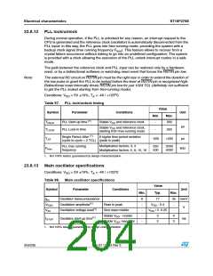
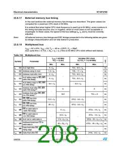
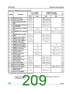
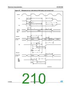
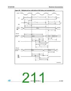
23.8.16 Memory cycle variables
The tables below use three variables which are derived from the BUSCONx registers and
represent the special characteristics of the programmed memory cycle. Table 103 describes
how these variables are computed.
Table 103. Memory cycle variables
Symbol
Description
ALE extension
Values
tA
tC
tF
TCL x [ALECTL]
Memory cycle time wait states
Memory tri-state time
2TCL x (15 - [MCTC])
2TCL x (1 - [MTTC])
Doc ID 12303 Rev 3
207/235

 STMICROELECTRONICS [ ST ]