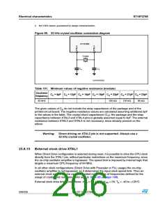
Electrical characteristics
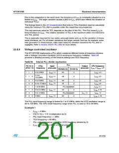
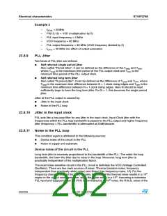
Example 2
ST10F276E
–
–
–
–
–
–
fXTAL = 8 MHz
P0(15:13) = ‘100’ (multiplication by 5)
PLL input frequency = 2 MHz
VCO frequency = 80 MHz
PLL output frequency = 40 MHz (VCO frequency divided by 2)
f
CPU = 40 MHz (no effect of output prescaler)
23.8.9
PLL Jitter
Two kinds of PLL jitter are defined:
●
Self referred single period jitter
Also called “Period Jitter”, it can be defined as the difference of the Tmax and Tmin
where Tmax is the maximum time period of the PLL output clock and Tmin is the
minimum time period of the PLL output clock.
,
●
Self referred long term jitter
Also called “N period jitter”, it can be defined as the difference of Tmax and Tmin, where
max is the maximum time difference between N + 1 clock rising edges and Tmin is the
T
minimum time difference between N + 1 clock rising edges. Here N should be kept
sufficiently large to have the long term jitter. For N = 1, this becomes the single period
jitter.
Jitter at the PLL output is caused by:
●
Jitter in the input clock
Noise in the PLL loop
●
23.8.10 Jitter in the input clock
PLL acts like a low pass filter for any jitter in the input clock. Input Clock jitter with the
frequencies within the PLL loop bandwidth is passed to the PLL output and higher frequency
jitter (frequency > PLL bandwidth) is attenuated at 20dB/decade.
23.8.11 Noise in the PLL loop
This condition again is attributed to the following sources:
●
Device noise of the circuit in the PLL
Noise in supply and substrate
●
Device noise of the circuit in the PLL
Long term jitter is inversely proportional to the bandwidth of the PLL: The wider the loop
bandwidth, the lower the jitter due to noise in the loop. Moreover, long term jitter is
practically independent of the multiplication factor.
The most noise sensitive circuit in the PLL circuit is definitely the VCO (Voltage Controlled
Oscillator). There are two main sources of noise: Thermal (random noise, frequency
independent thus practically white noise) and flicker (low frequency noise, 1/f). For the
frequency characteristics of the VCO circuitry, the effect of the thermal noise results in a 1/f2
region in the output noise spectrum, while the flicker noise in a 1/f3. Assuming a noiseless
PLL input and supposing that the VCO is dominated by its 1/f2 noise, the R.M.S. value of the
202/235
Doc ID 12303 Rev 3

 STMICROELECTRONICS [ ST ]