ST10F276E
Electrical characteristics
Due to this adaptation to the input clock, the frequency of fCPU is constantly adjusted so it is
locked to fXTAL. The slight variation causes a jitter of fCPU which also effects the duration of
individual TCLs.
The timings listed in the AC characteristics that refer to TCLs therefore must be calculated
using the minimum TCL that is possible under the respective circumstances.
The real minimum value for TCL depends on the jitter of the PLL. The PLL tunes fCPU to
keep it locked on fXTAL. The relative deviation of TCL is the maximum when it is referred to
one TCL period.
This is especially important for bus cycles using wait states and e.g. for the operation of timers,
serial interfaces, etc. For all slower operations and longer periods (such as, for example, pulse
train generation or measurement, lower baud rates) the deviation caused by the PLL jitter is
negligible. Refer to Section 23.8.9: PLL Jitter for more details.
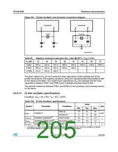
23.8.8
Voltage controlled oscillator
The ST10F276E implements a PLL which combines different levels of frequency dividers
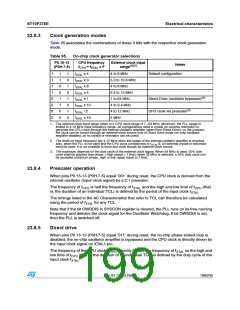
with a Voltage Controlled Oscillator (VCO) working as frequency multiplier. Table 96
presents a detailed summary of the internal settings and VCO frequency.
Table 96. Internal PLL divider mechanism
PLL
P0.15-13
(P0H.7-5)
XTAL
Input
Output
CPU frequency
frequency
prescaler
prescaler fCPU = fXTAL x F
Multiply by Divide by
1
1
1
1
1
0
4 to 8 MHz
fXTAL / 4
fXTAL / 4
64
48
4
4
-
-
fXTAL x 4
fXTAL x 3
5.3 to
10.6 MHz
1
1
0
0
0
0
0
0
1
1
0
0
1
0
1
0
1
0
4 to 8 MHz
6.4 to 12 MHz
1 to 64 MHz
4 to 6.4 MHz
4 to 12 MHz
4 MHz
fXTAL / 4
fXTAL / 4
-
64
40
2
2
-
fXTAL x 8
fXTAL x 5
-
PLL bypassed
-
fXTAL x 1
f
XTAL / 2
-
40
2
-
fXTAL x 10
fXTAL / 2
PLL bypassed
fPLL / 2
-
f
XTAL / 2
64
2
fXTAL x 16
The PLL input frequency range is limited to 1 to 3.5 MHz, while the VCO oscillation range is
64 to 128 MHz. The CPU clock frequency range when PLL is used is 16 to 64 MHz.
Example 1
–
–
–
–
–
–
fXTAL = 4 MHz
P0(15:13) = ‘110’ (multiplication by 3)
PLL input frequency = 1 MHz
VCO frequency = 48 MHz
PLL output frequency = 12 MHz (VCO frequency divided by 4)
f
CPU = 12 MHz (no effect of output prescaler)
Doc ID 12303 Rev 3
201/235

 STMICROELECTRONICS [ ST ]