Electrical characteristics
ST10F276E
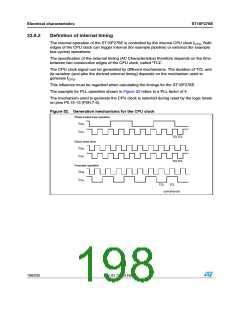
Therefore, the timings given in this chapter refer to the minimum TCL. This minimum value
can be calculated by the following formula:
TCL
= 1 ⁄ fXTALlxlDC
min
min
DC = duty cycle
For two consecutive TCLs, the deviation caused by the duty cycle of fXTAL is compensated,
so the duration of 2TCL is always 1/fXTAL
.
The minimum value TCLmin is used only once for timings that require an odd number of
TCLs (1, 3, ...). Timings that require an even number of TCLs (2, 4, ...) may use the formula:
2TCL= 1 ⁄ f
XTAL
The address float timings in multiplexed bus mode (t11 and t45) use the maximum duration of
TCL (TCLmax = 1/fXTAL x DCmax) instead of TCLmin
.
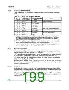
Similarly to what happens for Prescaler Operation, if the bit OWDDIS in SYSCON register is
cleared, the PLL runs on its free-running frequency and delivers the clock signal for the
Oscillator Watchdog. If bit OWDDIS is set, then the PLL is switched off.
23.8.6
Oscillator watchdog (OWD)
An on-chip watchdog oscillator is implemented in the ST10F276E. This feature is used for
safety operation with an external crystal oscillator (available only when using direct drive
mode with or without prescaler, so the PLL is not used to generate the CPU clock
multiplying the frequency of the external crystal oscillator). This watchdog oscillator
operates as following.
The reset default configuration enables the watchdog oscillator. It can be disabled by setting
the OWDDIS (bit 4) of SYSCON register.
When the OWD is enabled, the PLL runs at its free-running frequency and it increments the
watchdog counter. On each transition of external clock, the watchdog counter is cleared. If
an external clock failure occurs, then the watchdog counter overflows (after 16 PLL clock
cycles).
The CPU clock signal is switched to the PLL free-running clock signal and the oscillator
watchdog Interrupt Request is flagged. The CPU clock will not switch back to the external
clock even if a valid external clock exits on XTAL1 pin. Only a hardware reset (or
bidirectional Software / Watchdog reset) can switch the CPU clock source back to direct
clock input.
When the OWD is disabled, the CPU clock is always the external oscillator clock (in Direct
Drive or Prescaler Operation) and the PLL is switched off to decrease consumption supply
current.
23.8.7
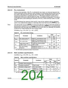
Phase locked loop (PLL)
For all other combinations of pins P0.15-13 (P0H.7-5) during reset the on-chip phase locked
loop is enabled and it provides the CPU clock (see Table 95). The PLL multiplies the input
frequency by the factor F which is selected via the combination of pins P0.15-13 (fCPU
=
fXTAL x F). With every F’th transition of fXTAL the PLL circuit synchronizes the CPU clock to
the input clock. This synchronization is done smoothly, so the CPU clock frequency does not
change abruptly.
200/235
Doc ID 12303 Rev 3

 STMICROELECTRONICS [ ST ]