NAND128-A, NAND256-A, NAND512-A, NAND01G-A
DC AND AC PARAMETERS
This section summarizes the operating and mea-
surement conditions, and the DC and AC charac-
teristics of the device. The parameters in the DC
and AC characteristics Tables that follow, are de-
rived from tests performed under the Measure-
ment
Conditions
summarized
in
Table
16., Operating and AC Measurement Conditions.
Designers should check that the operating condi-
tions in their circuit match the measurement condi-
tions when relying on the quoted parameters.
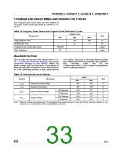
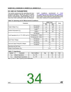
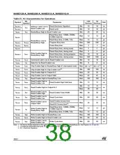
Table 16. Operating and AC Measurement Conditions
NAND Flash
Parameter
Units
Min
Max
1.95
3.6
70
1.8V devices
1.7
2.7
0
V
V
Supply Voltage (V
)
DD
3V devices
Grade 1
°C
°C
pF
pF
pF
V
Ambient Temperature (T )
A
Grade 6
–40
85
1.8V devices
3V devices (2.7 - 3.6V)
3V devices (3.0 - 3.6V)
1.8V devices
3V devices
30
50
Load Capacitance (C ) (1 TTL GATE and C )
L
L
100
V
0
DD
Input Pulses Voltages
0.4
2.4
V
1.8V devices
3V devices
0.9
1.5
5
V
Input and Output Timing Ref. Voltages
Input Rise and Fall Times
V
ns
kΩ
Output Circuit Resistors, R
8.35
ref
Table 17. Capacitance
Symbol
Parameter
Input Capacitance
Test Condition
Typ
Max
Unit
pF
C
V
IN
= 0V
= 0V
10
10
IN
C
I/O
V
IL
Input/Output Capacitance
pF
Note: TA = 25°C, f = 1 MHz. CIN and CI/O are not 100% tested.
34/57

 STMICROELECTRONICS [ ST ]