NAND128-A, NAND256-A, NAND512-A, NAND01G-A
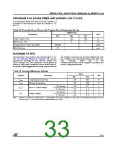
PROGRAM AND ERASE TIMES AND ENDURANCE CYCLES
The Program and Erase times and the number of
Program/ Erase cycles per block are shown in Ta-
ble 14.
Table 14. Program, Erase Times and Program Erase Endurance Cycles
NAND Flash
Parameters
Unit
Min
Typ
200
2
Max
500
3
Page Program Time
Block Erase Time
µs
ms
Program/Erase Cycles (per block)
Data Retention
100,000
10
cycles
years
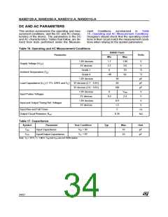
MAXIMUM RATING
Stressing the device above the ratings listed in Ta-
ble 15., Absolute Maximum Ratings, may cause
permanent damage to the device. These are
stress ratings only and operation of the device at
these or any other conditions above those indicat-
ed in the Operating sections of this specification is
not implied. Exposure to Absolute Maximum Rat-
ing conditions for extended periods may affect de-
vice
reliability.
Refer
also
to
the
STMicroelectronics SURE Program and other rel-
evant quality documents.
Table 15. Absolute Maximum Ratings
Value
Symbol
Parameter
Temperature Under Bias
Unit
Min
– 50
– 65
– 0.6
– 0.6
– 0.6
– 0.6
Max
125
150
2.7
T
BIAS
°C
°C
V
T
STG
Storage Temperature
Input or Output Voltage
1.8V devices
3 V devices
1.8V devices
3 V devices
(1)
V
IO
4.6
V
2.7
V
V
Supply Voltage
DD
4.6
V
Note: 1. Minimum Voltage may undershoot to –2V for less than 20ns during transitions on input and I/O pins. Maximum voltage may over-
shoot to VDD + 2V for less than 20ns during transitions on I/O pins.
33/57

 STMICROELECTRONICS [ ST ]