NAND128-A, NAND256-A, NAND512-A, NAND01G-A
SOFTWARE ALGORITHMS
This section gives information on the software al-
gorithms that ST recommends to implement to
manage the Bad Blocks and extend the lifetime of
the NAND device.
attempts to program or erase them will give errors
in the Status Register.
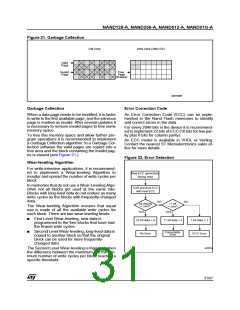
As the failure of a page program operation does
not affect the data in other pages in the same
block, the block can be replaced by re-program-
ming the current data and copying the rest of the
replaced block to an available valid block. The
Copy Back Program command can be used to
copy the data to a valid block.
See the “Copy Back Program” section for more de-
tails.
Refer to Table 13. for the recommended proce-
dure to follow if an error occurs during an opera-
tion.
NAND Flash memories are programmed and
erased by Fowler-Nordheim tunneling using a high
voltage. Exposing the device to a high voltage for
extended periods can cause the oxide layer to be
damaged. For this reason, the number of program
and erase cycles is limited (see Table 14. for val-
ue) and it is recommended to implement Garbage
Collection, a Wear-Leveling Algorithm and an Er-
ror Correction Code, to extend the number of pro-
gram and erase cycles and increase the data
retention.
To help integrate a NAND memory into an applica-
tion ST Microelectronics can provide:
Table 13. Block Failure
Operation
Erase
Recommended Procedure
Block Replacement
Block Replacement or ECC
ECC
■
File System OS Native reference software,
which supports the basic commands of file
management.
Program
Read
Contact the nearest ST Microelectronics sales of-
fice for more details.
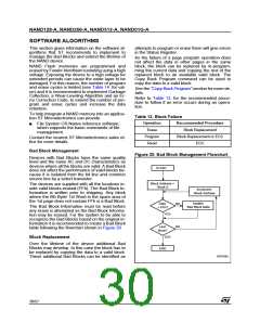
Bad Block Management
Figure 20. Bad Block Management Flowchart
Devices with Bad Blocks have the same quality
level and the same AC and DC characteristics as
devices where all the blocks are valid. A Bad Block
does not affect the performance of valid blocks be-
cause it is isolated from the bit line and common
source line by a select transistor.
The devices are supplied with all the locations in-
side valid blocks erased (FFh). The Bad Block In-
formation is written prior to shipping. Any block
where the 6th Byte/ 1st Word in the spare area of
the 1st page does not contain FFh is a Bad Block.
START
Block Address =
Block 0
Increment
Block Address
Update
Bad Block table
Data
NO
NO
The Bad Block Information must be read before
any erase is attempted as the Bad Block Informa-
tion may be erased. For the system to be able to
recognize the Bad Blocks based on the original in-
formation it is recommended to create a Bad Block
table following the flowchart shown in Figure 20.
= FFh?
YES
Last
block?
YES
Block Replacement
Over the lifetime of the device additional Bad
Blocks may develop. In this case the block has to
be replaced by copying the data to a valid block.
These additional Bad Blocks can be identified as
END
AI07588C
30/57

 STMICROELECTRONICS [ ST ]