2 Megabit Multi-Purpose Flash
SST39SF020
Preliminary Specifications
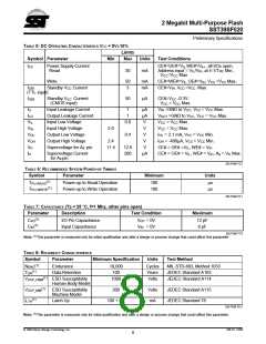
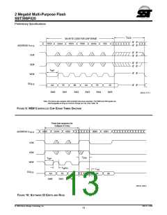
AC CHARACTERISTICS
TABLE 9: READ CYCLE TIMING PARAMETERS VCC = 4.5-5.5V
1
SST39SF020-70 SST39SF020-90
Symbol
TRC
Parameter
Min
Max
Min
Max
Units
ns
2
Read Cycle time
70
90
TCE
Chip Enable Access Time
Address Access Time
70
70
35
90
90
45
ns
TAA
ns
3
TOE
Output Enable Access Time
CE# Low to Active Output
OE# Low to Active Output
CE# High to High-Z Output
OE# High to High-Z Output
Output Hold from Address Change
ns
(1)
TCLZ
0
0
0
0
ns
(1)
TOLZ
ns
4
(1)
TCHZ
15
15
20
20
ns
(1)
TOHZ
ns
5
(1)
TOH
0
0
ns
326 PGM T9.2
Note: CL = 100 pF for 90 ns, CL = 30 pF for 70 ns
6
TABLE 10: PROGRAM/ERASE CYCLE TIMING PARAMETERS
7
Symbol
TBP
Parameter
Min
Max
Units
Byte Program time
Address Setup Time
Address Hold Time
WE# and CE# Setup Time
WE# and CE# Hold Time
OE# High Setup Time
OE# High Hold Time
CE# Pulse Width
30
µs
ns
ns
ns
ns
ns
ns
ns
ns
ns
ns
ns
ns
ns
ms
8
TAS
0
30
0
TAH
TCS
9
TCH
0
TOES
TOEH
TCP
0
10
11
12
13
14
15
16
0
40
40
30
30
30
0
TWP
WE# Pulse Width
TWPH (1)
TCPH (1)
TDS
WE# Pulse Width High
CE# Pulse Width High
Data Setup Time
TDH (1)
TIDA (1)
TSE
Data Hold Time
Software ID Access and Exit Time
Sector Erase
150
10
TSCE
Chip Erase
20
ms
326 PGM T10.4
Note: (1)This parameter is measured only for initial qualification and after the design or process change that could affect this parameter.
© 1998 Silicon Storage Technology, Inc.
326-10 12/98
9

 SST [ SILICON STORAGE TECHNOLOGY, INC ]