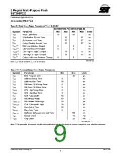
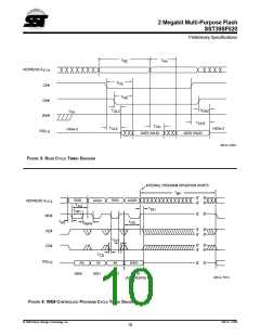
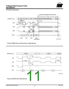
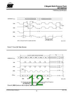
2 Megabit Multi-Purpose Flash
SST39SF020
Preliminary Specifications
TABLE 5: DC OPERATING CHARACTERISTICS VCC = 5V±10%
Limits
Symbol Parameter
Min
Max
Units
Test Conditions
ICC
Power Supply Current
Read
CE#=OE#=VIL,WE#=VIH , all I/Os open,
Address input = VIL/VIH, at f=1/TRC Min.,
VCC=VCC Max
30
mA
Write
50
3
mA
mA
CE#=WE#=VIL, OE#=VIH, VCC =VCC Max.
CE#=VIH, VCC =VCC Max.
ISB1
(TTL input)
Standby VCC Current
ISB2
Standby VCC Current
(CMOS input)
50
µA
CE#=VCC -0.3V.
VCC = VCC Max.
ILI
Input Leakage Current
Output Leakage Current
Input Low Voltage
1
1
µA
µA
V
VIN =GND to VCC, VCC = VCC Max.
VOUT =GND to VCC, VCC = VCC Max.
VCC = VCC Max.
ILO
VIL
VIH
VOL
VOH
VH
IH
0.8
Input High Voltage
Output Low Voltage
Output High Voltage
Supervoltage for A9 pin
2.0
V
VCC = VCC Max.
0.4
V
IOL = 2.1 mA, VCC = VCC Min.
IOH = -400µA, VCC = VCC Min.
CE# = OE# =VIL, WE# = VIH
CE# = OE# = VIL, WE# = VIH, A9 = VH Max.
2.4
V
11.4
12.6
200
V
Supervoltage Current
for A9 pin
µA
326 PGM T5.2
TABLE 6: RECOMMENDED SYSTEM POWER-UP TIMINGS
Symbol
Parameter
Minimum
Units
(1)
TPU-READ
Power-up to Read Operation
Power-up to Write Operation
100
100
µs
µs
(1)
TPU-WRITE
326 PGM T6.1
TABLE 7: CAPACITANCE (Ta = 25 °C, f=1 Mhz, other pins open)
Parameter
Description
Test Condition
Maximum
(1)
CI/O
I/O Pin Capacitance
Input Capacitance
VI/O = 0V
VIN = 0V
12 pF
6 pF
(1)
CIN
326 PGM T7.0
Note: (1)This parameter is measured only for initial qualification and after a design or process change that could affect this parameter.
TABLE 8: RELIABILITY CHARACTERISTICS
Symbol
Parameter
Minimum Specification
Units
Test Method
(1)
NEND
Endurance
10,000
100
Cycles
Years
Volts
MIL-STD-883, Method 1033
JEDEC Standard A103
JEDEC Standard A114
(1)
TDR
Data Retention
(1)
VZAP_HBM
ESD Susceptibility
Human Body Model
1000
(1)
VZAP_MM
ESD Susceptibility
Machine Model
200
Volts
mA
JEDEC Standard A115
JEDEC Standard 78
(1)
ILTH
Latch Up
100 + ICC
326 PGM T8.3
Note: (1)This parameter is measured only for initial qualification and after a design or process change that could affect this parameter.
© 1998 Silicon Storage Technology, Inc.
326-10 12/98
8

 SST [ SILICON STORAGE TECHNOLOGY, INC ]