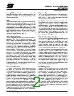
2 Megabit Multi-Purpose Flash
SST39SF020
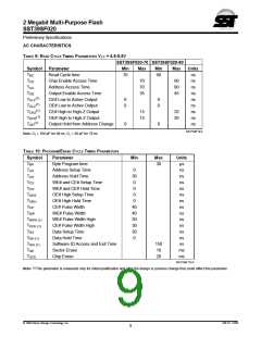
Preliminary Specifications
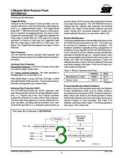
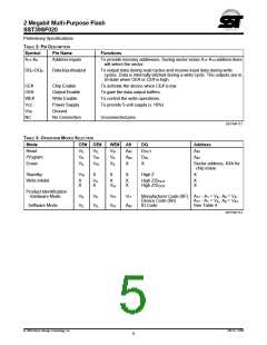
TABLE 2: PIN DESCRIPTION
Symbol
Pin Name
Functions
A17-A0
Address Inputs
To provide memory addresses. During sector erase A17-A12 address lines
will select the sector.
1
DQ7-DQ0
Data Input/output
To output data during read cycles and receive input data during write
cycles. Data is internally latched during a write cycle. The outputs are in
tri-state when OE# or CE# is high.
2
CE#
OE#
WE#
Vcc
Vss
NC
Chip Enable
Output Enable
Write Enable
Power Supply
Ground
To activate the device when CE# is low.
To gate the data output buffers.
To control the write operations.
To provide 5-volt supply (± 10%)
3
4
No Connection
Unconnected pins.
326 PGM T2.1
5
TABLE 3: OPERATION MODES SELECTION
6
Mode
Read
CE# OE#
WE# A9
DQ
DOUT
DIN
X
Address
AIN
VIL
VIL
VIL
VIL
VIH
VIH
VIH
VIL
VIL
AIN
AIN
X
7
Program
Erase
AIN
Sector address, XXh for
chip erase
8
Standby
VIH
X
X
X
High Z
X
Write Inhibit
X
X
VIL
X
X
VIH
X
X
High Z/DOUT
High Z/DOUT
X
X
9
Product Identification
Hardware Mode
VIL
VIL
VIL
VIL
VIH
VIH
VH
Manufacturer Code (BF) A17 - A1 = VIL, A0 = VIL
Device Code (B6)
ID Code
A17 - A1 = VIL, A0 = VIH
See Table 4
Software Mode
AIN
10
11
12
13
14
15
16
326 PGM T3.4
© 1998 Silicon Storage Technology, Inc.
326-10 12/98
5

 SST [ SILICON STORAGE TECHNOLOGY, INC ]