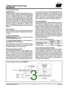
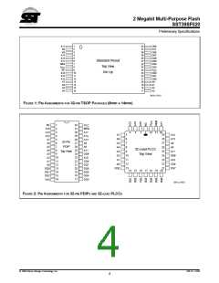
2 Megabit Multi-Purpose Flash
SST39SF020
Preliminary Specifications
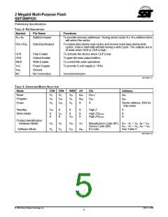
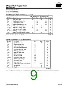
TABLE 4: SOFTWARE COMMAND SEQUENCE
Command
Sequence
1st Bus
Write Cycle
Addr(1) Data Addr(1) Data
2nd Bus
Write Cycle
3rd Bus
Write Cycle
Addr(1) Data Addr(1) Data
4th Bus
Write Cycle
5th Bus
Write Cycle
Addr(1) Data Addr(1) Data
6th Bus
Write Cycle
Byte Program
Sector Erase
Chip Erase
5555H AAH
5555H AAH
5555H AAH
2AAAH 55H
2AAAH 55H
2AAAH 55H
2AAAH 55H
5555H A0H
5555H 80H
5555H 80H
5555H 90H
BA(3)
Data
5555H AAH
5555H AAH
2AAAH 55H SAx(2) 30H
2AAAH 55H 5555H 10H
Software ID Entry 5555H AAH
Software ID Exit
Software ID Exit
XXH
F0H
5555H AAH
2AAAH 55H
5555H F0H
326 PGM T4.0
Notes:
(1)
Address format A14-A0 (Hex), Addresses A15, A16 and A17 are a “Don’t Care” for the
Command sequence.
SAx for sector erase; uses A17-A12 address lines
BA = Program Byte address
(2)
(3)
(4)
Both Software ID Exit operations are equivalent
Notes for Software ID Entry Command Sequence
1. With A17 -A1 =0; SST Manufacturer Code = BFH, is read with A0 = 0,
SST39SF020 Device Code = B6H, is read with A0 = 1.
2. The device does not remain in Software Product ID Mode if powered down.
© 1998 Silicon Storage Technology, Inc.
326-10 12/98
6

 SST [ SILICON STORAGE TECHNOLOGY, INC ]