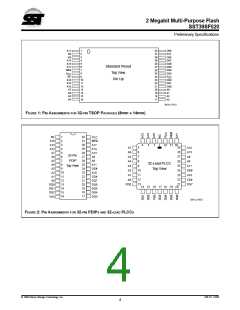
2 Megabit Multi-Purpose Flash
SST39SF020
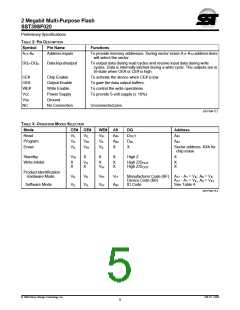
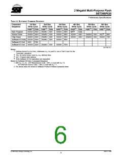
Preliminary Specifications
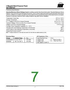
Absolute Maximum Stress Ratings (Applied conditions greater than those listed under “Absolute Maximum Stress
Ratings”maycausepermanentdamagetothedevice. Thisisastressratingonlyandfunctionaloperationofthedevice
at these conditions or conditions greater than those defined in the operational sections of this data sheet is not implied.
Exposure to absolute maximum stress rating conditions may affect device reliability.)
1
Temperature Under Bias ................................................................................................................. -55°C to +125°C
Storage Temperature ...................................................................................................................... -65°C to +150°C
D. C. Voltage on Any Pin to Ground Potential ............................................................................. -0.5V to VCC+ 0.5V
Transient Voltage (<20 ns) on Any Pin to Ground Potential......................................................... -1.0V to VCC+ 1.0V
Voltage on A9 Pin to Ground Potential ................................................................................................ -0.5V to 14.0V
Package Power Dissipation Capability (Ta = 25°C) ........................................................................................... 1.0W
Through Hole Lead Soldering Temperature (10 Seconds) .............................................................................. 300°C
Surface Mount Lead Soldering Temperature (3 Seconds) ............................................................................... 240°C
2
3
4
Output Short Circuit Current(1) ............................................................................................................................................................... 100 mA
Note: (1) Outputs shorted for no more than one second. No more than one output shorted at a time.
5
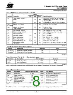
OPERATING RANGE
Range
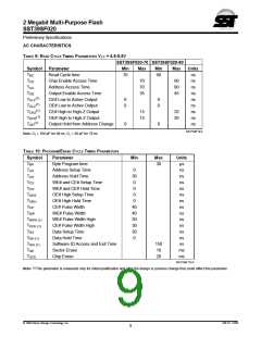
AC CONDITIONS OF TEST
6
Ambient Temp
0 °C to +70 °C
-40 °C to +85 °C
VCC
Input Rise/Fall Time......... 10 ns
Output Load..................... CL = 100 pF for 90 ns
Output Load..................... CL = 30 pF for 70 ns
See Figures 12 and 13
Commercial
Industrial
5V±10%
5V±10%
7
8
9
10
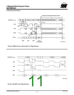
11
12
13
14
15
16
© 1998 Silicon Storage Technology, Inc.
326-10 12/98
7

 SST [ SILICON STORAGE TECHNOLOGY, INC ]