A d v a n c e I n f o r m a t i o n
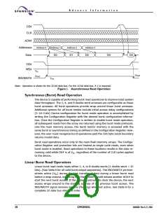
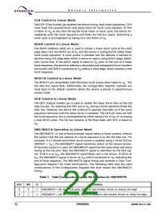
CE#
CLK
ADV#
Addresses
Address 0
Address 1
Address 2
Address 3
D0
D1
D2
D3
D3
Data
OE#
WE#
VIH
Float
Float
VOH
IND/WAIT#
Note: Operation is shown for the 32-bit data bus. For the 16-bit data bus, A-1 is required.
Figure 1. Asynchronous Read Operation
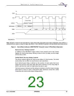
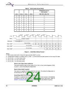
Synchronous (Burst) Read Operation
The device is capable of performing burst read operations to improve total system
data throughput. The 2, 4, and 8 double word accesses are configurable as linear
burst accesses. All burst operations provide wrap around linear burst accesses.
Additional options for all burst modes include initial access delay configurations
(2–16 CLKs) Device configuration for burst mode operation is accomplished by
writing the Configuration Register with the desired burst configuration informa-
tion. Once the Configuration Register is written to enable burst mode operation,
all subsequent reads from the array are returned using the burst mode protocols.
Like the main memory access, the SecSi Sector memory is accessed with the
same burst or asynchronous timing as defined in the Configuration Register. How-
ever, the user must recognize burst operations past the 256 byte SecSi boundary
returns invalid data.
Burst read operations occur only to the main flash memory arrays. The Configu-
ration Register and protection bits are treated as single cycle reads, even when
burst mode is enabled. Read operations to these locations results in the data re-
maining valid while OE# is at V , regardless of the number of CLK cycles applied
IL
to the device.
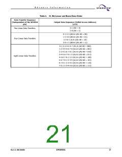
Linear Burst Read Operations
Linear burst read mode reads either 2, 4, or 8 double words (1 double word = 32
bits). (See Table 6 for all valid burst output sequences). The IND/WAIT# pin tran-
sitions active (V ) during the last transfer of data during a linear burst read
IL
before a wrap around, indicating that the system should initiate another ADV# to
start the next burst access. If the system continues to clock the device, the next
access wraps around to the starting address of the previous burst access. The
IND/WAIT# signal remains inactive (floating) when not active. See Table 6 for a
complete 32 data bus interface order.
20
S29CD032G
30606B0 March 22, 2004

 SPANSION [ SPANSION ]