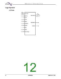
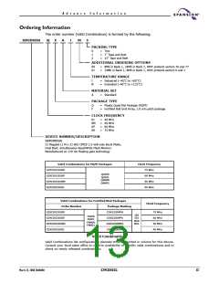
A d v a n c e I n f o r m a t i o n
it is not tested by executing an embedded operation in the big (busy) bank while
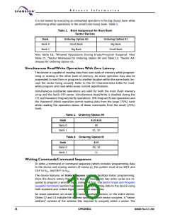
performing other operations in the small (non-busy) bank. Table 2.
Table 2. Bank Assignment for Boot Bank
Sector Devices
Bank
Bank 0
Bank 1
Ordering Option 00
Small Bank
Ordering Option 01
Big Bank
Big Bank
Small Bank
Also Table 18. ”Allowed Operations During Erase/Program Suspend. Also
Table 12. ”Sector Addresses for Ordering Option 00 and Table 13. ”Sector Ad-
dresses for Ordering Option 01.
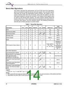
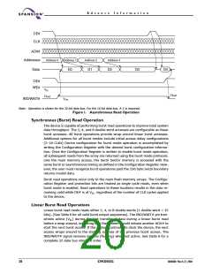
Simultaneous Read/Write Operations With Zero Latency
The device is capable of reading data from one bank of memory while program-
ming or erasing in the other bank of memory. An erase operation may also be
suspended to read from or program to another location within the same bank (ex-
cept the sector being erased). Refer to the DC Characteristics table for read-
while-program and read-while-erase current specifications.
Simultaneous read/write operations are valid for both the main Flash memory
array and the SecSi OTP sector. Simultaneous Read/Write is disabled during the
CFI and Password Program/Verify operations. PPB Program/Erase operations and
the Password Unlock operation permit reading data from the large (75%) bank
while reading the operation status of these commands from the small (25%)
bank.
Table 3. Ordering Option 00
Bank
Bank 0
Bank 1
A19:A18
00
01, 1X
Table 4. Ordering Option 01
Bank
A19
Bank 0
Bank 1
0X, 10
11
Writing Commands/Command Sequences
To write a command or command sequence (which includes programming data
to the device and erasing sectors of memory), the system must drive WE# and
CE# to V , and OE# to V .
IL
IH
The device features an Unlock Bypass mode to facilitate faster programming.
Once the device enters the Unlock Bypass mode, only two write cycles are re-
quired to program a word or byte, instead of four. The Sector Erase and Program
Suspend Command section has details on programming data to the device using
both standard and Unlock Bypass command sequences.
An erase operation can erase one sector, multiple sectors, or the entire device.
Tables 12 and 13 indicate the address space that each sector occupies. A “sector
address” consists of the address bits required to uniquely select a sector. The
16
S29CD032G
30606B0 March 22, 2004

 SPANSION [ SPANSION ]