A d v a n c e I n f o r m a t i o n
CE# Control in Linear Mode
The CE# (Chip Enable) pin enables the device during read mode operations. CE#
must meet the required burst read setup times for burst cycle initiation. If CE#
is taken to V at any time during the burst linear or burst cycle, the device im-
IH
mediately exits the burst sequence and floats the DQ bus signal. Restarting a
burst cycle is accomplished by taking CE# and ADV# to V .
IL
ADV# Control In Linear Mode
The ADV# (Address Valid) pin is used to initiate a linear burst cycle at the clock
edge when CE# and ADV# are at V and the device is configured for either linear
IL
burst mode operation. A burst access is initiated and the address is latched on
the first rising CLK edge when ADV# is active or upon a rising ADV# edge, which-
ever occurs first. If the ADV# signal is taken to V prior to the end of a linear
IL
burst sequence, the previous address is discarded and subsequent burst transfers
are invalid until ADV# transitions to V before a clock edge, which initiates a new
IH
burst sequence.
RESET# Control in Linear Mode
The RESET# pin immediately halts the linear burst access when taken to V . The
IL
DQ data bus signal float. Additionally, the Configuration Register contents are
reset back to the default condition where the device is placed in asynchronous
access mode.
OE# Control in Linear Mode
The OE# (Output Enable) pin is used to enable the linear burst data on the DQ
data bus pin. De-asserting the OE# pin to V during a burst operation floats the
IH
data bus. However, the device will continue to operate internally as if the burst
sequence continues until the linear burst is complete. The OE# pin does not halt
the burst sequence, this is accomplished by either taking CE# to V or re-issuing
IH
a new ADV# pulse. The DQ bus remains in the float state until OE# is taken to
V .
IL
IND/WAIT# Operation in Linear Mode
The IND/WAIT#, or End of Burst Indicator signal (when in linear modes), informs
the system that the last address of a burst sequence is on the DQ data bus. For
example, if a 2-double-word linear burst access is enabled using a 16-bit DQ bus
(WORD# = V ), the IND/WAIT# signal transitions active on the second access.
IL
If the same scenario is used, the IND/WAIT# signal has the same delay and setup
timing as the DQ pins. Also, the IND/WAIT# signal is controlled by the OE# sig-
nal. If OE# is at V , the IND/WAIT# signal floats and is not driven. If OE#is at
IH
V , the IND/WAIT# signal is driven at V until it transitions to V indicating the
IL
IH
IL
end of burst sequence. The IND/WAIT# signal timing and duration is (See “Con-
figuration Register” for more information). The following table lists the valid
combinations of the Configuration Register bits that impact the IND/WAIT#
timing.
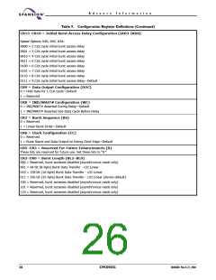
Table 7. Valid Configuration Register Bit Definition for IND/WAIT#
DOC
WC
0
CC
1
Definition
0
0
IND/WAIT# = VIL for 1-CLK cycle, Active on last transfer, Driven on risiong CLD edge
IND/WAIT# = VIL for 1-CLK cycle, Active on second to last transfer, Driven on rising CLK edge
1
1
22
S29CD032G
30606B0 March 22, 2004

 SPANSION [ SPANSION ]