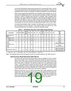
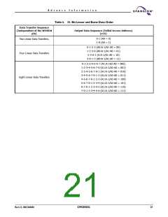
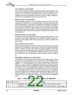
A d v a n c e I n f o r m a t i o n
V
V
IH
CE#
CLK
IL
3 Clock Delay
ADV#
Addresses
Data
Address 1 Latched
Address 1
Address 2
Invalid
D1
D2
D3
D0
OE#
IND/WAIT#
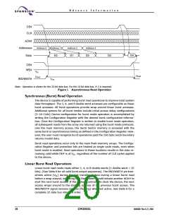
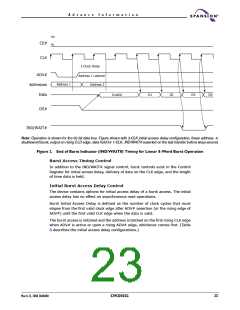
Note: Operation is shown for the 32-bit data bus. Figure shown with 3-CLK initial access delay configuration, linear address, 4-
doubleword burst, output on rising CLD edge, data hold for 1-CLK, IND/WAIT# asserted on the last transfer before wrap-around.
Figure 2. End of Burst Indicator (IND/WAIT#) Timing for Linear 8-Word Burst Operation
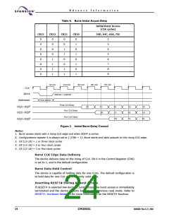
Burst Access Timing Control
In addition to the IND/WAIT# signal control, burst controls exist in the Control
Register for initial access delay, delivery of data on the CLK edge, and the length
of time data is held.
Initial Burst Access Delay Control
The device contains options for initial access delay of a burst access. The initial
access delay has no effect on asynchronous read operations.
Burst Initial Access Delay is defined as the number of clock cycles that must
elapse from the first valid clock edge after ADV# assertion (or the rising edge of
ADV#) until the first valid CLK edge when the data is valid.
The burst access is initiated and the address is latched on the first rising CLK edge
when ADV# is active or upon a rising ADV# edge, whichever comes first. (Table
8 describes the initial access delay configurations.)
March 22, 2004 30606B0
S29CD032G
23

 SPANSION [ SPANSION ]