A d v a n c e I n f o r m a t i o n
“Command Definitions” section has details on erasing a sector or the entire chip,
or suspending/resuming the erase operation.
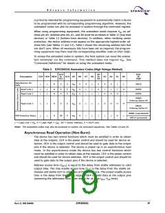
After the system writes the autoselect command sequence, the device enters the
autoselect mode. The system can then read autoselect codes from the internal
register (which is separate from the memory array) on DQ7–DQ0. Standard read
cycle timing applies in this mode. Refer to the “Autoselect Mode” section for more
information.
I
and I
in the DC Characteristics table represents the active current speci-
CC2
CC3
fication for erase or program modes. The AC Characteristics section contains
timing specification tables and timing diagrams for erase or program operations.
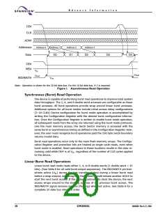
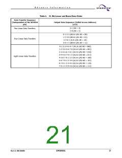
When in Synchronous read mode configuration, the device is able to perform both
asynchronous and synchronous write operations. CLK and ADV# address latch is
supported in synchronous programming mode. During a synchronous write oper-
ation, to write a command or command sequence, (which includes programming
data to the device and erasing sectors of memory), the system must drive ADV#
and CE# to VIL, and OE# to VIH when providing an address to the device, and
drive WE# and CE# to VIL, and CE# to VIH, when writing commands or data.
Accelerated Program and Erase Operations
The device offers accelerated program/erase operations through the ACC pin.
When the system asserts V (12V) on the ACC pin, the device automatically en-
HH
ters the Unlock Bypass mode. The system may then write the two-cycle Unlock
Bypass program command sequence to do accelerated programming. The device
uses the higher voltage on the ACC pin to accelerate the operation. A sector that
is being protected with the WP# pin will still be protect during accelerated pro-
gram or Erase. Note that the ACC pin must not be at V
during any operation
HH
other than accelerated programming, or device damage may result.
Autoselect Functions
If the system writes the autoselect command sequence, the device enters the au-
toselect mode. The system can then read autoselect codes from the internal
register (which is separate from the memory array) on DQ7–DQ0. Standard read
cycle timings apply in this mode. Refer to the Autoselect Mode and Autoselect
Command Sequence sections for more information.
Automatic Sleep Mode (ASM)
The automatic sleep mode minimizes Flash device energy consumption. While in
asynchronous mode, the device automatically enables this mode when addresses
remain stable for t
+ 60 ns. The automatic sleep mode is independent of the
ACC
CE#, WE# and OE# control signals. Standard address access timings provide
new data when addresses are changed. While in sleep mode, output data is
latched and always available to the system. While in synchronous mode, the de-
vice automatically enables this mode when either the first active CLK level is
greater than t
or the CLK runs slower than 5 MHz. Note that a new burst op-
ACC
eration is required to provide new data.
I
in the “DC Characteristics” section represents the automatic sleep mode cur-
CC8
rent specification.
Standby Mode
When the system is not responding or writing to the device, it can place the de-
vice in the standby mode. In this mode, current consumption is greatly reduced,
March 22, 2004 30606B0
S29CD032G
17

 SPANSION [ SPANSION ]