A d v a n c e I n f o r m a t i o n
is primarily intended for programming equipment to automatically match a device
to be programmed with its corresponding programming algorithm. However, the
autoselect codes can also be accessed in-system through the command register.
When using programming equipment, the autoselect mode requires V on ad-
ID
dress pin A9. Address pins A6, A1, and A0 must be as shown in Table 12 (top boot
devices) or Table 13 (bottom boot devices). In addition, when verifying sector
protection, the sector address must appear on the appropriate highest order ad-
dress bits (see Tables 12 and 13). Table 5 shows the remaining address bits that
are don’t care. When all necessary bits have been set as required, the program-
ming equipment may then read the corresponding identifier code on DQ7–DQ0.
To access the autoselect codes in-system, the host system can issue the autose-
lect command via the command. This method does not require V . See
ID
“Command Definitions” for details on using the autoselect mode.
Table 5. S29CD032G Autoselect Codes (High Voltage Method)
A19
to
A11
A5
to
A4
DQ7
to
DQ0
Description
CE# OE# WE#
A10
A9
A8
A7
A6
A3
A2
A1
A0
Manufacturer ID:
FASL
L
L
H
X
X
V
X
X
L
X
X
X
L
L
0001h
ID
Read Cycle 1
Read Cycle 2
L
L
L
L
H
H
X
X
X
X
V
V
X
X
L
L
L
L
X
L
L
L
L
H
L
007Eh
0009h
ID
ID
H
H
H
0000h
Ordering Option 00
Read Cycle 3
L
L
L
L
H
H
X
X
X
V
V
X
X
L
L
L
L
L
L
H
L
H
L
H
H
H
L
ID
ID
0001h
Ordering Option 01
0000h (unprotected)
0001h (protected)
PPB Protection Status
SA
L = Logic Low = V , H = Logic High = V
, SA = Sector Address, X = Don’t care.
IL
IH
Note: The autoselect codes may also be accessed in-system via command sequences. See Tables 18 and 20.
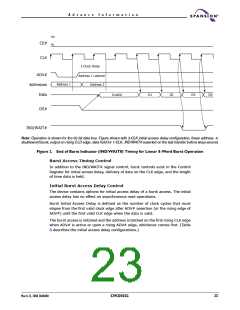
Asynchronous Read Operation (Non-Burst)
The device has two control functions which must be satisfied in order to obtain
data at the outputs. CE# is the power control and should be used for device se-
lection. OE# is the output control and should be used to gate data to the output
pins if the device is selected. The device is power-up in an asynchronous read
mode. In the asynchronous mode the device has two control functions which
must be satisfied in order to obtain data at the outputs. CE# is the power control
and should be used for device selection. OE# is the output control and should be
used to gate data to the output pins if the device is selected.
Address access time (t
) is equal to the delay from stable addresses to valid
ACC
output data. The chip enable access time (t ) is the delay from the stable ad-
CE
dresses and stable CE# to valid data at the output pins. The output enable access
time is the delay from the falling edge of OE# to valid data at the output pins
(assuming the addresses have been stable for at least t
–t time).
ACC OE
March 22, 2004 30606B0
S29CD032G
19

 SPANSION [ SPANSION ]