A d v a n c e I n f o r m a t i o n
and the outputs are placed in the high impedance state, independent of the OE#
input.
The device enters the CMOS standby mode when the CE# and RESET# inputs are
both held at Vcc 0.2 V. The device requires standard access time (t ) for read
CE
access, before it is ready to read data.
If the device is deselected during erasure or programming, the device draws ac-
tive current until the operation is completed.
I
in the “DC Characteristics” section represents the standby current
CC5
specification.
Caution: entering the standby mode via the RESET# pin also resets the device
to the read mode and floats the data I/O pins. Furthermore, entering I
during
CC7
a program or erase operation will leave erroneous data in the address locations
being operated on at the time of the RESET# pulse. These locations require up-
dating after the device resumes standard operations. Refer to the “RESET#:
Hardware Reset Pin” section for further discussion of the RESET# pin and its
functions.
RESET#: Hardware Reset Pin
The RESET# pin is an active low signal that is used to reset the device under any
circumstances. A logic “0” on this pin forces the device out of any mode that is
currently executing back to the reset state. The RESET# pin may be tied to the
system reset circuitry. A system reset would thus also reset the device. To avoid
a potential bus contention during a system reset, the device is isolated from the
DQ data bus by tristating the data output pins for the duration of the RESET
pulse. All pins are “don’t care” during the reset operation.
If RESET# is asserted during a program or erase operation, the RY/BY# pin re-
mains low until the reset operation is internally complete. This action requires
between 1 µs and 7µs for either Chip Erase or Sector Erase. The RY/BY# pin can
be used to determine when the reset operation is complete. Otherwise, allow for
the maximum reset time of 11 µs. If RESET# is asserted when a program or erase
operation is not executing (RY/BY# = “1”), the reset operation will complete
within 500 ns. The Simultaneous Read/Write feature of this device allows the user
to read a bank after 500 ns if the bank was in the read/reset mode at the time
RESET# was asserted. If one of the banks was in the middle of either a program
or erase operation when RESET# was asserted, the user must wait 11 µs before
accessing that bank.
Asserting RESET# during a program or erase operation leaves erroneous data
stored in the address locations being operated on at the time of device reset.
These locations need updating after the reset operation is complete. See Figure
19 for timing specifications.
Asserting RESET# active during V
and V power-up is required to guarantee
IO
CC
proper device initialization until V
voltages.
and V have reached their steady state
IO
CC
Output Disable Mode
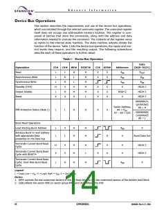
See Table 1 Device Bus Operation for OE# Operation in Output Disable Mode.
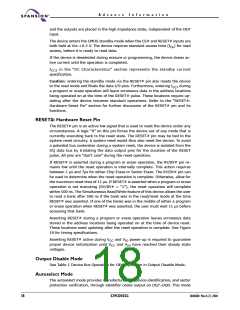
Autoselect Mode
The autoselect mode provides manufacturer and device identification, and sector
protection verification, through identifier codes output on DQ7–DQ0. This mode
18
S29CD032G
30606B0 March 22, 2004

 SPANSION [ SPANSION ]