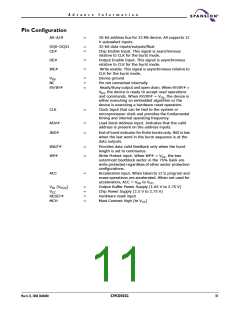
A d v a n c e I n f o r m a t i o n
VersatileI/O™ (V ) Control
IO
The VersatileI/O (V ) control allows the host system to set the voltage levels that
IO
the device generates at its data outputs and the voltages tolerated at its data in-
puts to the same voltage level that is asserted on the V pin.
IO
The output voltage generated on the device is determined based on the V
IO
(V
) level.
CCQ
A V of 1.65–1.95 volts is targeted to provide for I/O tolerance at the 1.8 volt
IO
level.
A V and V of 2.5–2.75 volts makes the device appear as 2.5 volt-only.
CC
IO
Requirements for Reading Array Data
To read array data from the outputs, the system must drive the CE# and OE#
pins to V . CE# is the power control and selects the device. OE# is the output
IL
control and gates array data to the output pins. WE# should remain at V .
IH
The internal state machine is set for reading array data upon device power-up,
or after a hardware reset. This ensures that no spurious alteration of the memory
content occurs during the power transition. No command is necessary in this
mode to obtain array data. Standard microprocessor read cycles that assert valid
addresses on the device address inputs produce valid data on the device data
outputs. The device remains enabled for read access until the command register
contents are altered.
Address access time (t
) is the delay from stable addresses to valid output
ACC
data. The chip enable access time (t ) is the delay from stable addresses and
CE
stable CE# to valid data at the output pins. The output enable access time (t
)
OE
is the delay from the falling edge of OE# to valid data at the output pins (assum-
ing the addresses have been stable for at least t –t time and CE# has been
ACC OE
asserted for at least t –t time).
CE OE
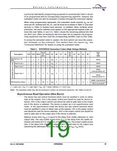
See “Reading Array Data” for more information. Refer to the AC Read Operations
table for timing specifications and to 15 for the timing diagram. I in the DC
CC1
Characteristics table represents the active current specification for reading array
data.
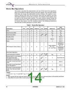
Simultaneous Read/Write
Operations Overview and Restrictions
Overview
The Simultaneous Read/Write feature allows a program or erase operation to be
executed in one (busy) bank, while performing other operations in the other bank
(non-busy).
The Simultaneous Read/Write operation of this device has been optimized for ap-
plications that could most benefit from this capability. These applications store
code in the larger bank, while storing data in the smaller bank. The best example
of this is when a Sector Erase Operation (as an embedded operation) in the
smaller (busy) bank, while performing a Burst/synchronous Read Operation in
the larger (non-busy) bank.
Restrictions
The Simultaneous Read/Write function is tested by executing an embedded op-
eration in the small (busy) bank while performing other operations in the big
(non-busy) bank. However, the opposite case is neither tested nor valid. That is,
March 22, 2004 30606B0
S29CD032G
15

 SPANSION [ SPANSION ]