A d v a n c e I n f o r m a t i o n
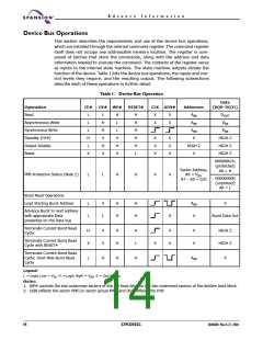
Device Bus Operations
This section describes the requirements and use of the device bus operations,
which are initiated through the internal command register. The command register
itself does not occupy any addressable memory location. The register is com-
posed of latches that store the commands, along with the address and data
information needed to execute the command. The contents of the register serve
as inputs to the internal state machine. The state machine outputs dictate the
function of the device. Table 1 lists the device bus operations, the inputs and con-
trol levels they require, and the resulting output. The following subsections
describe each of these operations in further detail.
Table 1. Device Bus Operation
Data
Operation
Read
CE#
OE#
L
WE#
RESET#
CLK
X
ADV#
Addresses
(DQ0–DQ31)
L
L
H
L
H
H
H
H
H
L
X
X
A
A
A
D
OUT
IN
IN
IN
Asynchronous Write
Synchronous Write
Standby (CE#)
Output Disable
Reset
H
X
D
IN
IN
L
H
L
D
H
L
X
X
H
X
X
X
X
X
X
X
X
HIGH Z
HIGH Z
HIGH Z
H
HIGH Z
X
X
X
00000001h,
(protected)
A6 = H
Sector Address,
PPB Protection Status (Note 2)
L
L
H
H
X
X
A9 = V ,
ID
00000000h
(unprotect)
A6 = L
A7 – A0 = 02h
Burst Read Operations
Load Starting Burst Address
L
L
X
L
H
H
H
H
A
X
IN
Advance Burst to next address
with appropriate Data
H
X
Burst Data Out
presented on the Data bus
Terminate Current Burst Read
Cycle
H
X
X
X
H
H
H
L
X
X
X
X
HIGH Z
HIGH Z
Terminate Current Burst Read
Cycle with RESET#
X
Terminate Current Burst Read
Cycle; Start New Burst Read
Cycle
L
H
H
H
A
X
IN
Legend:
L = Logic Low = V , H = Logic High = V , X = Don’t care.
IL
IH
Notes:
1. WP# controls the two outermost sectors of the top boot block or the two outermost sectors of the bottom boot block.
2. DQ0 reflects the sector PPB (or sector group PPB) and DQ1 reflects the DYB
14
S29CD032G
30606B0 March 22, 2004

 SPANSION [ SPANSION ]