CXD1185CQ/CR
PHC
: Phase Change
Indicates that the SCSI phase has been changed. This bit is set if the CXD1185C is operating in
the initiator mode and the target has changed the SCSI phase (MSG, I/O, C/D signal), and driven
REQ.
DATN : Drive ATN
Indicates that the SCSI bus ATN signal has been driven. This bit is set if the CXD1185C is
operating in the target mode and the initiator has driven the ATN signal.
: Data bus Parity Error
DPE
SPE
Indicates a parity error on the data bus. This bit is only set if environment setting register bit 5
(DPEN) is set to “1”. In initial status odd parity (environment register bit 6 set to “0”) is selected.
: SCSI bus Parity Error
Indicates a parity error on the SCSI bus. Parity check takes place during the selection phase and
data transfer phases.
RMSG : REQ in Message Phase
Indicates that the REQ signal has been driven during the message phase when the CXD1185C is in
initiator mode. This bit is used if two different batches of message data have been received during
the message phase or if the target requests the message to be resent.
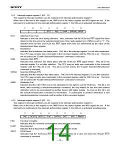
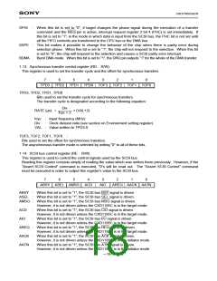
1-5. Environment setting register (R3 : W)
This register is used to set the operating mode of the CXD1185C.
Normally, some value must be written to this register immediately after a hardware reset from the CPU.
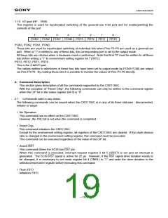
7
6
5
4
3
2
1
0
DIFE SDPM DPEN SIRM
FS1
FS0
DIFE : Selects the differential mode.
When this bit is set to “1”, general-use I/O port Pins P3-P0 are assigned for differential mode bits.
SDPM : Selects the data bus parity condition.
This bit is set to “0” for odd parity and to “1” for even parity. However, its value is irrelevant if the
DPEN bit is set to “0”.
DPEN : Enables parity generation/check for the data bus.
If this bit is set to “1”, data bus parity signal is input/output via the DP pin.
SIRM : Select the IRQ signal logic level.
After a hardware reset is performed, the IRQ signal output is positive logic. To change the IRQ
signal to negative logic. “1” must be set in this bit. At this time, the logic level of MIRQ bit is not
affected.
FS1, FS0 :
Used to select the CXD1185C clock division ratio.
The appropriate values, as shown in the table below, must be written into these bits to match the
external clock frequency applied to the CXD1185C :
Input frequency (MHz)
FS1
0
FS0
0
Clock division ratio
16-13
12-9
8-5
4
3
2
0
1
1
For the changes made to these bits , “Chip Reset” command must be executed.
Bits FS1 and FS0 are set for a clock division ratio of “4” after a hardware reset.
—15—

 SONY [ SONY CORPORATION ]