CXD1185CQ/CR
SPHI : When this bit is set to “0”, if target changes the phase signal during the execution of a transfer
command and the REQ pin is active, interrupt request register 2 bit 4 (PHC) is set immediately. If
this bit is set to “1”, in the mode in which data is input from the SCSI bus, the PHC bit is not set until
all the FIFO contents are transferred to the CPU bus or the DMA bus.
SSPE : This bit makes it possible to change the behavior of the chip when there is parity error during
selection phase. When this bit is set to “1”, the chip will not respond to the selection. When this bit
is set to “0”, the chip will respond to the selection and causes a SCSI parity error interrupt.
BDMA : Burst DMA mode. When this bit is set to “1”, the DRQ pin outputs “1” for the whole of the DMA transfer.
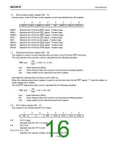
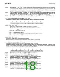
1-13. Synchronous transfer control register (RD : R/W)
This register is used to set the transfer cycle and the offset for synchronous transfers.
7
6
5
4
3
2
1
0
TPD3 TPD2 TPD1 TPD0 TOF3 TOF2 TOF1 TOF0
TPD3, TPD2, TPD1, TPD0
:
Bits used to set the transfer cycle for synchronous transfers.
The transfer cycle is designated according to the following equation :
Div
fcyc × 2
RATE (µs) =
× (VAL+2)
fcyc : Input frequency (MHz)
Div : Clock division ratio (see section on Environment setting register)
VAL : Value written to TPD3-0
TOF3, TOF2, TOF1, TOF0
:
Bits used to set the offset for synchronous transfers.
The asynchronous transfer mode is selected by writing “0” to all of these bits.
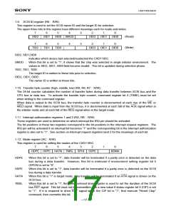
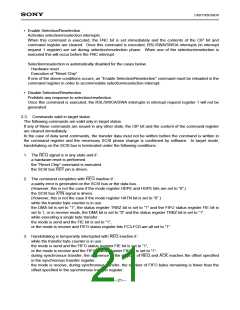
1-14. SCSI bus control register (RE : R/W)
This register is used to control the control signals used by the SCSI bus.
Reading this register consists simply of reading the value which was written there previously. However, if the
“Assert SCSI Control” command is executed, “0”s will be read out. The “Assert SCSI Control” command
must be executed in order to output this register’s value to the SCSI bus.
7
6
5
4
3
2
1
0
ABSY ASEL AMSG ACD
AIO
AREQ AACK AATN
ABSY : When this bit is set to “1”, the SCSI bus BSY signal is driven.
ASEL : When this bit is set to “1”, the SCSI bus SEL signal is driven.
AMSG : When this bit is set to “1”, the SCSI bus MSG signal is driven.
However, it is not driven unless the CXD1185C is in the target mode.
ACD
: When this bit is set to “1”, the SCSI bus C/D signal is driven.
However, it is not driven unless the CXD1185C is in the target mode.
: When this bit is set to “1”, the SCSI bus I/O signal is driven.
However, it is not driven unless the CXD1185C is in the target mode.
AIO
AREQ : When this bit is set to “1”, the SCSI bus REQ signal is driven.
However, it is not driven unless the CXD1185C is in the target mode.
AACK : When this bit is set to “1”, the SCSI bus ACK signal is driven.
However, it is not driven unless the CXD1185C is in the initiator mode.
AATN : When this bit is set to “1”, the SCSI bus ATN signal is driven.
However, it is not driven unless the CXD1185C is in the initiator mode.
—18—

 SONY [ SONY CORPORATION ]