CXD1185CQ/CR
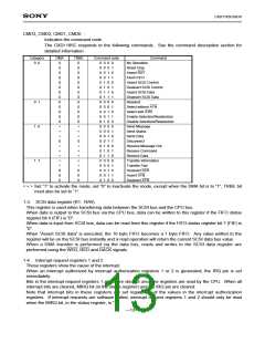
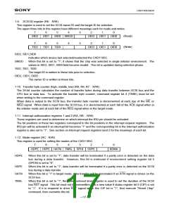
1-9. SCSI ID register (R6 : R/W)
This register is used to set the SCSI owner ID and the target ID for selection.
The upper three bits in this register have different meanings each for reads and writes.
7
6
5
4
3
2
1
0
(Read)
(Write)
SID2
SID1
SID0 SMOD
OID2
OID1
OID0
7
6
5
4
3
2
1
0
TID2
TID1
TID0
OID2
OID1
OID0
SID2, SID1,SID0
:
Indicates which device last selected/reselected the CXD1185C.
SMOD : When this bit is set to “1”, it shows that the chip was selected in single initiator environment. The
values in SID2, SID1, SID0 field become invalid. This bit is updated during selection phase.
TID2, TID1, TID0
The target ID is written to these bits prior to selection.
OID2, OID1, OID0 :
:
The owner ID is written to these bits.
1-10. Transfer byte counter (high, middle, low) (R9, R8, R7 : R/W)
The 24-bit counter calculates the number of transfer bytes during data transfer between SCSI bus and the
CPU bus or data bus. To activate the transfer byte counter, command register bit 4 (TRBE) must be set
when writing to the command register.
When data is output to the SCSI bus, the transfer byte counter is decremented at each rise of the WE or
WED signal. When data is input from the SCSI bus, it is decremented at each fall of the ACK signal when in
the initiator mode and at each fall of the REQ signal when in the target mode.
1-11. Interrupt authorization registers 1 and 2 (RA, RB : R/W)
These registers are used to determine on which interrupt the IRQ pin should be activated.
The bit positions in these two registers correspond to the bit positions in the interrupt request registers. The
IRQ pin will be activated if an interrupt bit becomes “1” and the corresponding bit in the interrupt authorization
register is also set to “1”. See section on Interrupt request registers land 2 for the meanings of each bit.
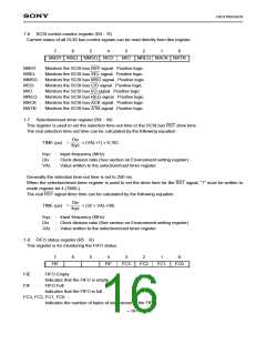
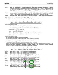
1-12. Mode register (RC : R/W)
This register is used for setting the modes of the CXD1185C.
7
6
5
4
3
2
1
0
HDPE HSPE HATN TMSL SPHI SSPE
BDMA
HDPE : When this bit is set to “1”, data transfer will be terminated if a parity error is detected on the data
bus during a data transfer. However, this bit is irrelevant if environment setting register bit 5
(DPEN) is set to “0”.
HSPE : When this bit is set to “1”, data transfer will be terminated if a parity error is detected on the SCSI
bus during a data transfer.
HATN : When this bit is “1” in target mode, data transfer will be terminated if an ATN signal is driven on the
SCSI bus.
TMSL : When this bit is set to “1”, the selection/reset timer register is used to set the duration of the SCSI
bus RST signal. This bit must not be overwritten with a new value if status register bit 0 (CIP) is set
to “1”. If it is required to drive RST signal when the CIP bit is “1”, first execute “Reset Chip”
command, then overwrite this bit.
—17—

 SONY [ SONY CORPORATION ]