CXD1185CQ/CR
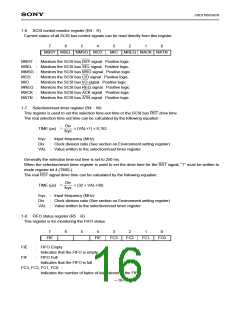
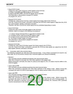
1-6. SCSI control monitor register (R4 : R)
Current status of all SCSI bus control signals can be read directly from this register.
7
6
5
4
3
2
1
0
MBSY MSEL MMSG MCD
MIO
MREQ MACK MATN
MBSY : Monitors the SCSI bus BSY signal. Positive logic.
MSEL : Monitors the SCSI bus SEL signal. Positive logic.
MMSG : Monitors the SCSI bus MSG signal. Positive logic.
MCD : Monitors the SCSI bus C/D signal. Positive logic.
MIO
: Monitors the SCSI bus I/O signal. Positive logic.
MREQ : Monitors the SCSI bus REQ signal. Positive logic.
MACK : Monitors the SCSI bus ACK signal. Positive logic.
MATN : Monitors the SCSI bus ATN signal. Positive logic.
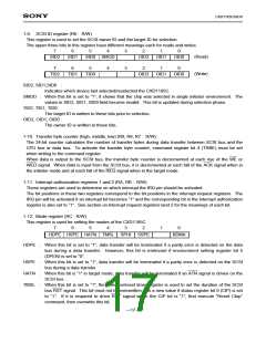
1-7. Selection/reset timer register (R4 : W)
This register is used to set the selection time-out time or the SCSI bus RST drive time.
The real selection time-out time can be calculated by the following equation :
Div
TIME (µs)
=
× (VAL+1) × 8,192
fcyc
fcyc : Input frequency (MHz)
Div : Clock division ratio (See section on Environment setting register)
VAL : Value written to the selection/reset timer register
Generally the selection time-out time is set to 250 ms.
When the selection/reset timer register is used to set the drive time for the RST signal, “1” must be written to
mode register bit 4 (TMSL).
The real RST signal drive time can be calculated by the following equation :
Div
TIME (µs)
=
× (32 × VAL+38)
fcyc
fcyc : Input frequency (MHz)
Div : Clock division ratio (See section on Environment setting register)
VAL : Value written to the selection/reset timer register
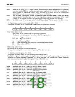
1-8. FIFO status register (R5 : R)
This register is for monitoring the FIFO status.
7
6
5
4
3
2
1
0
FIE
FIE
FC3
FC2
FC1
FC0
FIE
FIF
: FIFO Empty
Indicates that the FIFO is empty.
: FIFO Full
Indicates that the FIFO is full.
FC3, FC2, FC1, FC0 :
Indicates the number of bytes of data stored in the FIFO.
—16—

 SONY [ SONY CORPORATION ]