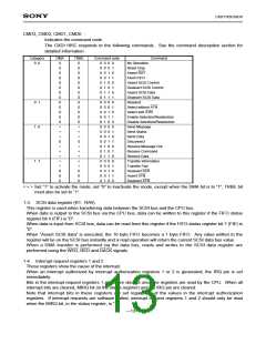
CXD1185CQ/CR
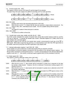
CMD3, CMD2, CMD1, CMD0 :
Indicates the command code.
The CXD1185C responds to the following commands. See the command description section for
detailed information.
Category
0 0
DMA
0
TRBE
Command code
0 0 0 0
0 0 0 1
0 0 1 0
0 0 1 1
0 1 0 0
0 1 0 1
0 1 1 0
0 1 1 1
0 0 0 0
0 0 0 1
0 0 1 0
0 0 1 1
0 1 0 0
0 0 0 0
0 0 0 1
0 0 1 0
0 0 1 1
0 1 0 0
0 1 0 1
0 1 1 0
0 0 0 0
0 0 0 1
0 0 1 0
0 0 1 1
0 1 0 0
Command
0
0
0
0
0
0
0
0
0
0
0
0
0
No Operation
Reset Chip
Assert RST
Flush FIFO
0
0
0
0
Assert SCSI Control
Deassert SCSI Control
Assert SCSI Data
Deassert SCSI Data
Reselect
0
0
0
0 1
0
0
Select without ATN
Select with ATN
Enable Selection/Reselection
Disable Selection/Reselection
Send Message
0
0
0
1 0
Send Status
Send Data
0
0
Disconnect
Receive Message Out
Receive Command
Receive Data
1 1
Transfer Information
Transfer Pad
0
0
0
0
0
0
Deassert ACK
Assert ATN
Deassert ATN
<
> Set “1” to activate the mode, set “0” to inactivate the mode, except when the DMA bit is to “1”, TRBE bit
must also be set to “1”.
1-3. SCSI data register (R1: R/W)
This register is used when transferring data between the SCSI bus and the CPU bus.
When data is output to the SCSI bus via the CPU bus, data can be written to this register if the FIFO status
register bit 4 (FIF) is “0”.
When data is input from SCSI bus, data can be read from this register if the FIFO status register bit 7 (FIE) is
“0”.
When “Assert SCSI data” is executed, the 16 byte FIFO becomes a 1 byte FIFO. Any value written to the
register will be on the SCSI bus instantly and a read operation will return the current SCSI data bus value.
When a DMA transfer is performed via the data bus, reads and writes to the SCSI data register are
performed using the WED, RED and DACK signals.
1-4. Interrupt request registers 1 and 2
These registers show the cause of the interrupt.
When an interrupt authorized by interrupt authorization registers 1 or 2 is generated, the IRQ pin is set
immediately.
Bits in the interrupt request registers 1 and 2 are cleared once the registers are read by the CPU. When all
interrupt bits are cleared, MIRQ bit (in the status register) and the IRQ pin are cleared.
Note that interrupt bits in these registers are set regardless of the values in the interrupt authorization
registers. If interrupt requests are software polled, interrupt request registers 1 and 2 should only be read
when the MIRQ bit, in the status register, is “1”.
—13—

 SONY [ SONY CORPORATION ]