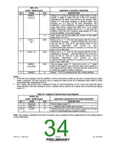
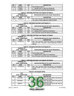
BIT
[7:2]
1
NAME
R/W
R
DESCRIPTION
This bit always reads “0”.
Reserved
512Bytes
COUNT8
R
1 = Indicates that 512 bytes were transferred
Bit 8 of the byte count for the data transferred.
0
R
Table 43 – RAM Buffer Write Byte Count Register B2 Register
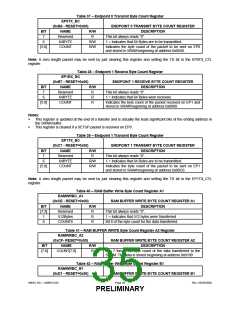
RAMWRBC_B2
RAM BUFFER WRITE BYTE COUNT REGISTER B2
(0xD2 - RESET=0x00)
NAME
BIT
R/W
DESCRIPTION
[7:0]
COUNT[7:0]
R
Bits 7 thru 0 the byte count of the data transferred to SRAM.
The packet is stored beginning at address 0x0300.
Table 44 – RAM Buffer Read Byte Count Register A1
RAMRDBC_A1
(0xD3 - RESET=0x00)
NAME
RAM BUFFER READ BYTE COUNT REGISTER A1
DESCRIPTION
BIT
[7:2]
1
R/W
R
Reserved
This bit always reads “0”.
512Bytes
R/W
R/W
1 = Indicates that 512 bytes are to transferred
Bit 8 of the byte count for the data to be transferred.
0
COUNT8
Table 45 – RAM Buffer Read Byte Count Register A2 Register
RAMRDBC_A2
(0xD4 - RESET=0x00)
NAME
RAM BUFFER READ BYTE COUNT REGISTER A2
DESCRIPTION
BIT
R/W
[7:0]
COUNT[7:0]
R/W
Bits 7 thru 0 the byte count of the packet to be transferred
from the SRAM. The packet is stored beginning at address
0x0100
Table 46 – RAM Buffer Read Byte Count Register B1
RAMRDBC_B1
(0xD5 - RESET=0x00)
NAME
RAM BUFFER READ BYTE COUNT REGISTER B1
DESCRIPTION
BIT
[7:2]
1
R/W
R
Reserved
This bit always reads “0”.
512Bytes
R/W
R/W
1 = Indicates that 512 bytes are to transferred
Bit 8 of the byte count for the data to be transferred.
0
COUNT8
Table 47 – RAM Buffer Read Byte Count Register B2 Register
RAMRDBC_B2
(0xD6 - RESET=0x00)
NAME
RAM BUFFER READ BYTE COUNT REGISTER B2
DESCRIPTION
BIT
R/W
[7:0]
COUNT[7:0]
R/W
Bits 7 thru 0 the byte count of the packet to be transferred
from the SRAM. The packet is stored beginning at address
0x0300.
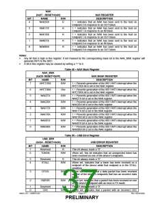
Table 48 – NAK Register (INT5)
NAK
(0xD7 - RESET=0x00)
NAME
NAK REGISTER
BIT
R/W
DESCRIPTION
7
NYET2RX
R
1 = indicates that an NYET has been sent to the host on
Endpoint 2 in response to an OUT token.
6
5
NYET0RX
NAK2TX
R
R
1 = indicates that an NYET has been sent to the host on
Endpoint 0 in response to an OUT token.
1 = indicates that an NAK has been sent to the host on
Endpoint 2 in response to an IN token.
SMSC DS – USB97C201
Page 36
Rev. 03/25/2002
PRELIMINARY

 SMSC [ SMSC CORPORATION ]