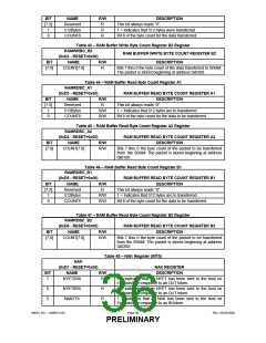
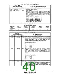
Table 58 –ATA Ultra DMA Timing Register
ATA_DMA
(0xDE - RESET=0x00)
NAME
ATA ULTRA DMA TIMING REGISTER
DESCRIPTION
BIT
[7:3]
[2:0]
R/W
R
Reserved
These bits always reads “0”.
DMA_TMG[2:0]
R/W
Drive Timing.
These bit settings the Ultra DMA mode that the ATA
interface operates when Ultra DMA operation is enabled.
They therefore determine the minimum data write strobe
Cycle Time (CT) and minimum Ready to Pause time (RP).
are shown below:
000: CT= 267ns, RP= 333ns (Mode 0)
001: CT= 167ns, RP= 266ns (Mode 1)
010: CT= 133ns, RP= 200ns (Mode 2)
011: CT= 100ns, RP= 200ns (Mode 3)
100: CT= 66ns, RP= 200ns (Mode 4)
101 thru 111 reserved
ULTRA DMA TIMING MODES
Mode (Data
Strobe
Mode 0
(~1267ns)
Mode 1
(~167ns)
Mode 2
(~133ns)
Mode 3
(~100ns)
Mode 4
(~66ns)
Cycle Time)
Bit Settings
000
001
010
011
100
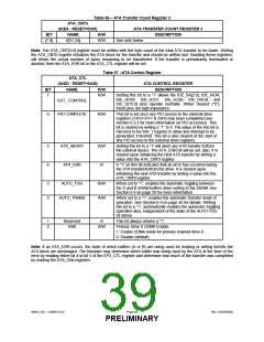
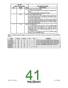
Table 59 – IDE Timing Register
IDE_TIM
(0xDF - RESET=0x00)
IDE TIMING REGISTER
DESCRIPTION
BIT
[7:6]
NAME
R/W
ISP[1:0]
R/W IORDY Sample Point. This field selects the number of 30MHz
clocks (33ns/clock) between IDE_nIOx assertion and the first
IORDY sample point. In fast PIO timing mode (See bit 3
below), this sets the active period for the data strobe.
Bits [7-6]Number of Clocks
00
01
10
11
5 clocks
4 clocks
3 clocks
2 clocks.
[5:4]
RT[0:1]
R/W Recovery Time. This field selects the minimum number of
30MHz clocks(33ns/clock) between the last IORDY sample
point and the next IDE_nIOx strobe. In fast PIO timing mode
(See bit 3 below), this sets the inactive period for the data
strobe.
Bits [5-4]Number of Clocks
00
01
10
11
4 clocks
3 clocks
2 clocks
1 clock.
3
DTE
R/W DMA Timing Enable Only.
1: Fast timing mode is enabled for non-UDMA DMA data. PIO
transfer to the IDE data port will run in compatible timing.
0: Both non-UDMA DMA and PIO data transfers to drive will
use the fast timing mode.
SMSC DS – USB97C201
Page 40
Rev. 03/25/2002
PRELIMINARY

 SMSC [ SMSC CORPORATION ]