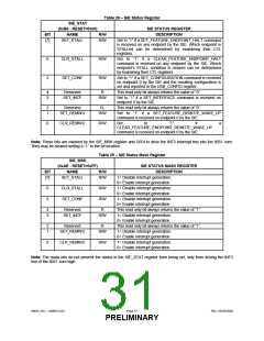
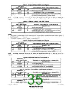
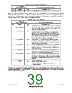
Table 37 – Endpoint 0 Transmit Byte Count Register
EP0TX_BC
(0xB6 - RESET=0x00)
NAME
ENDPOINT 0 TRANSMIT BYTE COUNT REGISTER
DESCRIPTION
BIT
7
R/W
R
Reserved
This bit always reads “0”.
6
64BYTE
R/W
R/W
1 = Indicates that 64 Bytes are to be transmitted.
[5:0]
COUNT
Indicates the byte count of the packet to be sent on EP0
and stored in SRAM beginning at address 0x0040.
Note: A zero length packet may be sent by just clearing this register and setting the TX bit in the EP0TX_CTL
register.
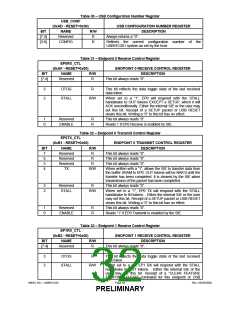
Table 38 – Endpoint 1 Receive Byte Count Register
EP1RX_BC
(0xB7 - RESET=0x00)
NAME
ENDPOINT 1 RECEIVE BYTE COUNT REGISTER
DESCRIPTION
BIT
7
R/W
R
Reserved
This bit always reads “0”.
6
64BYTE
R
1 = Indicates that 64 Bytes were received.
[5:0]
COUNT
R
Indicates the byte count of the packet received on EP1 and
stored in SRAM beginning at address 0x0080.
Notes:
ꢀ
This register is updated at the end of a transfer and is actually the least significant bits of the ending address in
the SRAM buffer.
ꢀ
This register is cleared if a SETUP packet is received on EP0.
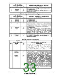
Table 39 – Endpoint 1 Transmit Byte Count Register
EP1TX_BC
(0xC7 - RESET=0x00)
NAME
ENDPOINT 1 TRANSMIT BYTE COUNT REGISTER
DESCRIPTION
BIT
7
R/W
R
Reserved
This bit always reads “0”.
6
64BYTE
R/W
R/W
1 = Indicates that 64 Bytes are to be transmitted.
[5:0]
COUNT
Indicates the byte count of the packet to be sent on EP1
and stored in SRAM beginning at address 0x00C0.
Note: A zero length packet may be sent by just clearing this register and setting the TX bit in the EP1TX_CTL
register.
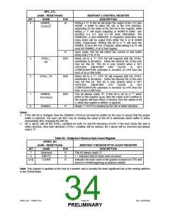
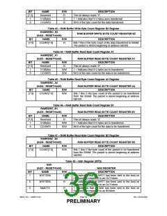
Table 40 – RAM Buffer Write Byte Count Register A1
RAMWRBC_A1
(0xCE - RESET=0x00)
NAME
RAM BUFFER WRITE BYTE COUNT REGISTER A1
DESCRIPTION
BIT
[7:2]
1
R/W
R
Reserved
This bit always reads “0”.
512Bytes
R
1 = Indicates that 512 bytes were transferred
Bit 8 of the byte count for the data transferred.
0
COUNT8
R
Table 41 – RAM BUFFER WRITE Byte Count Register A2 Register
RAMWRBC_A2
(0xCF- RESET=0x00)
NAME
RAM BUFFER WRITE BYTE COUNT REGISTER A2
DESCRIPTION
BIT
R/W
[7:0]
COUNT[7:0]
R
Bits 7 thru 0 the byte count of the data transferred to the
SRAM. The data is stored beginning at address 0x0100
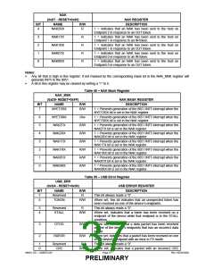
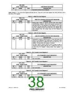
Table 42 – RAM Buffer Write Byte Count Register B1
RAMWRBC_B1
(0xD1 - RESET=0x00)
RAM BUFFER WRITE BYTE COUNT REGISTER B1
SMSC DS – USB97C201
Page 35
Rev. 03/25/2002
PRELIMINARY

 SMSC [ SMSC CORPORATION ]