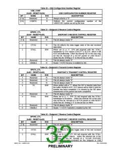
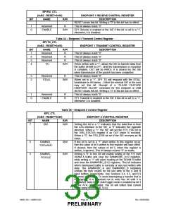
EP1RX_CTL
(0xB2 - RESET=0x00)
NAME
ENDPOINT 1 RECEIVE CONTROL REGISTER
BIT
R/W
DESCRIPTION
RESET clears this bit. Writing a “0” to this bit has no effect.
This bit always reads “0”.
1
0
Reserved
ENABLE
R
R/W
EP1 Receive is enabled in the SIE if this bit is set to a “1”,
otherwise, it is disabled.
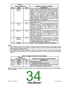
Table 34 – Endpoint 1 Transmit Control Register
EP1TX_CTL
(0xB3 - RESET=0x00)
NAME
ENDPOINT 1 TRANSMIT CONTROL REGISTER
DESCRIPTION
BIT
7
R/W
R
Reserved
Reserved
Reserved
TX
This bit always reads “0”.
6
R
This bit always reads “0”.
5
R
This bit always reads “0”.
4
R/W
When written with a “1”, allows the SIE to transfer data from
the buffer SRAM to EP1. Until the transmission or reception
is complete, OUT will be NAK’d. It is cleared by the SIE
when transmission of the packet has been completed.
3
2
Reserved
STALL
R
This bit always reads “0”.
R/W
When set to a “1”, EP1 TX will respond with the STALL
handshake to IN tokens. . Either the internal SIE or the user
may set this bit. Receipt of
a “CLEAR FEATURE
ENDPOINT CLEAR” command for this endpoint or USB
RESET clears this bit. Writing a “0” to this bit has no effect.
1
0
Reserved
ENABLE
R
R
This bit always reads “0”.
EP1 Transmit is enabled in the SIE if this bit is set to a “1”,
otherwise, it is disabled.
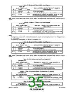
Table 35 – Endpoint 2 Control Register
EP2_CTL
(0xB4 - RESET=0x00)
NAME
ENDPOINT 2 CONTROL REGISTER
BIT
R/W
DESCRIPTION
7
DIR
R/W
Setting this bit to a “1” indicates that the data flow is from
the ATA interface to the SIE, a “0” indicates the opposite
direction. When a “1”, the SIE will set the EP2_ERR bit in
the USB_STATUS register if an OUT token is received.
When a “0”, the EP2_ERR bit set if the SIE receives an IN
token.
6
5
RAMWR_
TOGVALID
R/W
R/W
If this bit is set to a “1” when writes to this register occur,
then the value of bit 5 written to this register will have effect.
If cleared, then the values of bit 5, when this register is
written, is ignored. This bit always returns “0” on reads.
RAMWR_
TOGGLE
Writing a “0” to this bit will enable writing of the 512 byte
SRAM A buffer and clear the RAMWRBC_A1/2 registers,
while writing a “1” will select loading of the SRAM B buffer
and clear the RAMWRBC_B1/2 registers. This bit indicates
which interleaved buffer is currently or was last written with
data. The RAMWRBC_A and RAMWRBC_B Registers
contain the byte counts for the last write to the A and B
input buffers, respectively. See Sections 6.4, 6.5, and 6.9
for more information. To avoid interrupting a transfer that is
in progress, it is important not to write this bit until it is
completed. Note that if AutoToggle mode is enabled by bit 3
of the ATA_CTL register, this bit will reflect that current
buffer being written(1=B, 0=A).
SMSC DS – USB97C201
Page 33
Rev. 03/25/2002
PRELIMINARY

 SMSC [ SMSC CORPORATION ]