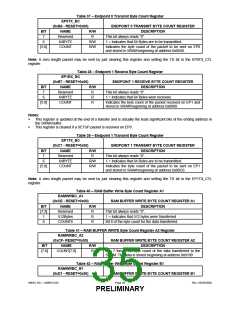
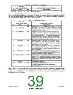
Table 56 – ATA Transfer Count Register 3
ATA_CNT3
(0xE4 - RESET=0x00)
NAME
ATA TRANSFER COUNT REGISTER 3
DESCRIPTION
BIT
R/W
[7:0]
D[31:24]
R/W
See note below.
Note: The ATA_CNT[3:0] register must be written with the byte count of the total ATA transfer to be made. Writing
the ATA_CNT0 register initializes the ATA block for the transfer and should be written last. Reading these registers,
will return the actual number of bytes remaining to be transferred. If the transfer is prematurely terminated or
aborted, then the ATA_ERR bit in the ATA_CTL register will be set.
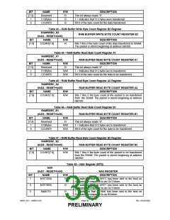
Table 57 –ATA Control Register
ATA_CTL
(0xDD - RESET=0x00)
NAME
ATA CONTROL REGISTER
DESCRIPTION
BIT
R/W
7
R/W
Setting this bit to a “1” allows the IDE_SA[2:0], IDE_nIOR,
IDE_nIOW, IDE_nCS1, IDE_nCS0, IDE_DACK, and
IDE_D[15:0] pins operate normally. When cleared (“0”),
these pins are high impedance.
OUT_ CONTROL
PIO COMPLETE
6
R/W
This bit is set once any PIO access to the external drive
registers (31F0-31F7 & 33F6) has been completed (see
Section 6.3.2 for more information on PIO accesses). This
bit is cleared by writing a “1” to it. The value of the this bit is
mirrored in the ISR_1 register to allow and interrupt to be
generated, if desired. This bit is also cleared at the start of
any PIO access to the external drive registers.
5
4
ATA_ABORT
ATA_ERR
R/W
R
Setting this bit to a “1” will abort any ATA transfer to/from
the external device. The ATA_ERR bit will be set, also. It is
cleared upon initializing the next ATA transfer by writing a
value into the ATA_CNT0 register.
A “1” on this bit indicates that an error has occurred during
the ATA transfer/to/from the drive. It is cleared upon
initializing the next ATA transfer by writing a value into the
ATA_CNT0 register.
3
2
AUTO_TOG
R/W
R/W
When set to “1”, enables the automatic toggling between
the A and B SRAM buffers when writing to the SRAM. See
Section 6.9 on page 50 for more information
AUTO_TRANS
When set to a “1”, enables the automatic transfer mode of
operation. See Section 6.9 on page 50 for details. Writing
this bit to a “1”, automatically enables the automatic toggling
operation also, independent of the state of the AUTO-TOG
bit above.
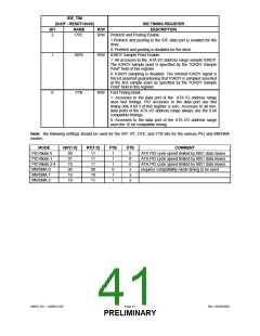
1
0
Reserved
EN0
R
This bit always returns a “1”.
R/W
Primary Drive 0 UDMA Enable.
1: Enable UDMA mode for primary channel drive 0.
0: Disable (default)..
Note: If an ATA_ERR occurs, the state of which buffers (A or B) are being used for reading or writing form/to the
ATA block are unchanged. The firmware may determine which buffer was being used by the ATA at the time of the
error by reading either bit 4 or bit 5 of the EP2_CTL register and determine how much of the transfer was completed
by reading the ATA_CNx registers.
SMSC DS – USB97C201
Page 39
Rev. 03/25/2002
PRELIMINARY

 SMSC [ SMSC CORPORATION ]