Advanced I/O Controller with Motherboard GLUE Logic
Datasheet
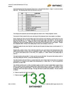
Data transmissions from the keyboard consist of an 11-bit serial data stream. A logic 1 is sent at an active
high level. The following table shows the functions of the bits.
BIT
1
2
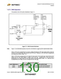
FUNCTION
Start bit (always 0)
Data bit 0 (least significant bit)
Data bit 1
3
4
5
Data bit 2
Data bit 3
6
Data bit 4
7
8
Data bit 5
Data bit 6
9
10
11
Data bit 7 (most significant bit)
Parity bit (odd parity)
Stop Bit (always 1)
The timing for the keyboard clock and data signals are shown in the “Timing Diagrams” section.
The process to find a match for the scan code stored in the Keyboard Scan Code register is as follows:
Begin sampling the data at the first falling edge of the keyboard clock following a period where the clock
line has been high for 115-145usec. The data at this first clock edge is the start bit. The first data bit
follows the start bit (clock 2). Sample the data on each falling edge of the clock. Store the eight bits
following the stop bit to compare with the scan code stored in the Keyboard Scan Code register. Sample
the comparator within 100usec of the falling edge of clock 9 (for example, at clock 10).
Sample the parity bit and check that the 8 data bits plus the parity bit always have an odd number of 1’s
(odd parity).
Repeat until a match is found. If the 8 data bits match the scan code stored in the Keyboard Scan Code
register and the parity is correct, then it is considered a match. When a match is found and if the stop bit
is 1, set the event status bit (bit 5 of the PME_STS1 register) to ‘1’ within 100usec of the falling edge of
clock 10.
The state machine will reset after 11 clocks and the process will restart. The process will continue until it is
shut off by setting the SPEKEY_EN bit (see following sub-section).
The state machine will reset if there is a period where the clock remains high for more than one keyboard
clock period (115-145usec) in the middle of the transmission (i.e., before clock 11). This is to prevent the
generation of a false PME.
The SPEKEY_EN bit at bit 1 of the CLOCKI32 register at 0xF0 in Power Control Block Logical Device
when LD_NUM=0 and the Runtime Register Block Logical Device when LD_NUM=1. This register is used
to control the “wake-on-specific feature. This bit is used to turn the logic for this feature on and off. It will
disable the 32kHz clock input to the logic. The logic will draw no power when disabled. The bit is defined
as follows:
0= “Wake on specific key” logic is on (default)
1= “Wake on specific key” logic is off
SMSC LPC47M182
133
Revision 1.8 SMSC/Non-SMSC Register Sets (02-24-05)
DATASHEET

 SMSC [ SMSC CORPORATION ]