Advanced I/O Controller with Motherboard GLUE Logic
Datasheet
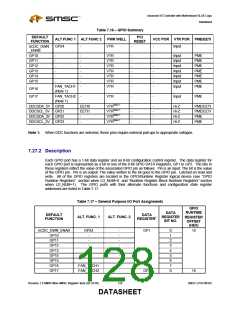
GPIO
RUNTIME
DATA
REGISTER
BIT NO.
DEFAULT
DATA
ALT. FUNC. 1
ALT. FUNC. 2
REGISTER
OFFSET
(HEX)
FUNCTION
REGISTER1
DDCSDA_5V
DDCSCL_5V
DDCSDA_3V
DDCSCL_3V
Reserved
GP20
GP21
GP22
GP23
-
EETI0
EETI1
1
2
3
4
7:5
-
-
-
Note 1: The GPIO Data and Configuration Registers are located in GPIO/Runtime Register block at the offset
shown from the GPIO/Runtime Register Block logical device base address.
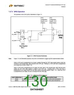
7.27.3 GPIO Control
Each GPIO port has an 8-bit control register that controls the behavior of the pin. (See “GPIO Runtime
Registers” section when LD_NUM=0 and “Runtime Register Block Runtime Registers” section when
LD_NUM=1).
Each GPIO port may be configured as either an input or an output. If the pin is configured as an output, it
can be programmed as open-drain or push-pull. Inputs and outputs can be configured as non-inverting or
inverting. Bit[0] of each GPIO Configuration Register determines the port direction, bit[1] determines the
signal polarity, and bit[7] detemines the output driver type select.
The Polarity Bit (bit 1) of the GPIO control registers control the GPIO pin when the pin is configured for the
GPIO function and when the pin is configured for the alternate function for all pins, with the exception of
the either edge triggered interrupts and DDC functions.
The basic GPIO configuration options are summarized in Table 7.18.
Table 7.18 – GPIO Configuration Summary
SELECTED
FUNCTION
DIRECTION
BIT
POLARITY
BIT
DESCRIPTION
B0
0
0
1
1
B1
0
1
0
1
Pin is a non-inverted output.
Pin is an inverted output.
Pin is a non-inverted input.
Pin is an inverted input.
GPIO
SMSC LPC47M182
129
Revision 1.8 SMSC/Non-SMSC Register Sets (02-24-05)
DATASHEET

 SMSC [ SMSC CORPORATION ]