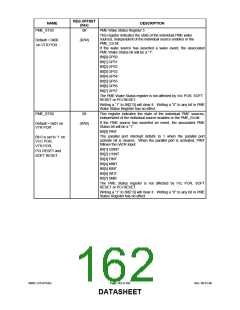
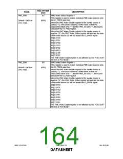
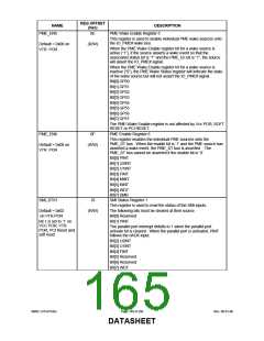
REG OFFSET
(hex)
NAME
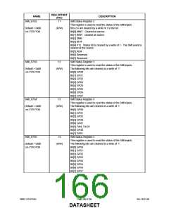
SMI_STS2
DESCRIPTION
11
SMI Status Register 2
This register is used to read the status of the SMI inputs.
Bits 2-6 are cleared by a write of 1 to the bit.
Bit[0] MINT. Cleared at source.
Bit[1] KINT. Cleared at source.
Bit[2] SMB
Default = 0x00
on VTR POR
(R/W)
Bit[3] RI1#
Bit[4] P12. Status bit is cleared by a write of 1. The SMI event is
cleared at the source.
Bit[5] RI2#
Bit[6] Reserved
Bit[7] Reserved
SMI_STS3
12
SMI Status Register 3
This register is used to read the status of the SMI inputs.
Default = 0x00
on VTR POR
(R/W)
The following bits are cleared on a write of ‘1’.
Bit[0] GP20
Bit[1] GP21
Bit[2] GP22
Bit[3] GP60
Bit[4] GP24
Bit[5] GP25
Bit[6] GP26
Bit[7] GP27
SMI_STS4
13
SMI Status Register 4
This register is used to read the status of the SMI inputs.
Default = 0x00
on VTR POR
(R/W)
The following bits are cleared on a write of ‘1’.
Bit[0] GP30
Bit[1] GP31
Bit[2] GP32
Bit[3] GP33
Bit[4] GP41
Bit[5] FAN_TACH
Bit[6] GP43
Bit[7] GP61
SMI_STS5
14
SMI Status Register 5
This register is used to read the status of the SMI inputs.
Default = 0x00
on VTR POR
(R/W)
The following bits are cleared on a write of ‘1’.
Bit[0] GP50
Bit[1] GP51
Bit[2] GP52
Bit[3] GP53
Bit[4] GP54
Bit[5] GP55
Bit[6] GP56
Bit[7] GP57
SMSC LPC47S45x
Page 166 of 259
Rev. 06-01-06
DATASHEET

 SMSC [ SMSC CORPORATION ]