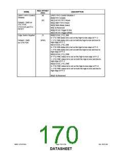
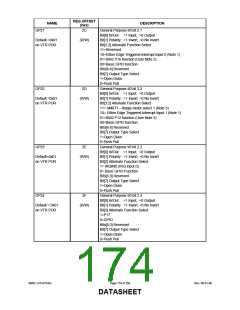
REG OFFSET
(hex)
NAME
DESCRIPTION
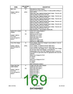
UART FIFO Control Shadow 1
UART1 FIFO Control
Shadow
20
Bit[0] FIFO Enable
(R)
Bit[1] RCVR FIFO Reset
Default = 0x00 on
VCC POR,
Bit[2] XMIT FIFO Reset
Bit[3] DMA Mode Select
Bit[5:4] Reserved
VTR POR and PCI
RESET
Bit[6] RCVR Trigger (LSB)
Bit[7] RCVR Trigger (MSB)
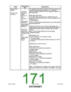
Bit[0] EDGE_P12_SMI
Edge Select Register
21
0= P12 SMI status bit is set on the high-to-low edge of P1.2
Default = 0x00
on VTR POR
(R/W)
1= P12 SMI status bit is set on both the high-to-low and low-to-
high edge of P1.2
Bit[1] EDGE_P16_SMI
0= P16 SMI status bit is set on the high-to-low edge of P1.6
1= P16 SMI status bit is set on both the high-to-low and low-to-
high edge of P1.6
Bit[2] EDGE_P12_PME
0= P12 PME status bit is set on the high-to-low edge of P1.2
1= P12 PME status bit is set on both the high-to-low and low-to-
high edge of P1.2
Bit[3] EDGE_P16_PME
0= P16 PME status bit is set on the high-to-low edge of P1.6
1= P16 PME status bit is set on both the high-to-low and low-to-
high edge of P1.6
Bits[7:4] Reserved
SMSC LPC47S45x
Page 170 of 259
Rev. 06-01-06
DATASHEET

 SMSC [ SMSC CORPORATION ]