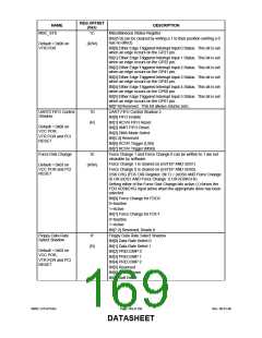
REG OFFSET
(hex)
NAME
MSC_STS
DESCRIPTION
Miscellaneous Status Register
1C
Bits[5:0] can be cleared by writing a 1 to their position (writing a 0
has no effect).
Default = 0x00 on
VTR POR
(R/W)
Bit[0] Either Edge Triggered Interrupt Input 0 Status. This bit is set
when an edge occurs on the GP21 pin.
Bit[1] Either Edge Triggered Interrupt Input 1 Status. This bit is set
when an edge occurs on the GP22 pin.
Bit[2] Either Edge Triggered Interrupt Input 2 Status. This bit is set
when an edge occurs on the GP41 pin.
Bit[3] Either Edge Triggered Interrupt Input 3 Status. This bit is set
when an edge occurs on the GP43 pin.
Bit[4] Either Edge Triggered Interrupt Input 4 Status. This bit is set
when an edge occurs on the GP60 pin.
Bit[5] Either Edge Triggered Interrupt Input 5 Status. This bit is set
when an edge occurs on the GP61 pin.
Bit[7:6] Reserved. This bit always returns zero.
UART FIFO Control Shadow 2
Bit[0] FIFO Enable
UART2 FIFO Control
Shadow
1D
(R)
Bit[1] RCVR FIFO Reset
Bit[2] XMIT FIFO Reset
Default = 0x00 on
VCC POR,
Bit[3] DMA Mode Select
VTR POR and PCI
RESET
Bit[5:4] Reserved
Bit[6] RCVR Trigger (LSB)
Bit[7] RCVR Trigger (MSB)
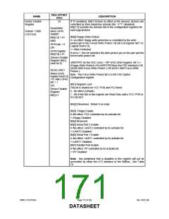
Force Disk Change
1E
Force Change 1 and Force Change 0 can be written to 1 are not
clearable by software.
Force Change 1 is cleared on (nSTEP AND nDS1)
Force Change 0 is cleared on (nSTEP AND nDS0).
Default = 0x03 on
VCC POR and PCI
RESET
(R/W)
DSK CHG (FDC DIR Register, Bit 7) = (nDS0 AND Force Change
0) OR (nDS1 AND Force Change 1) OR nDSKCHG.
Setting either of the Force Disk Change bits active (1) forces the
FDD nDSKCHG input active when the appropriate drive has been
selected.
Bit[0] Force Change for FDC0
0=Inactive
1=Active
Bit[1] Force Change for FDC1
0=Inactive
1=Active
Bit[7:2] Reserved, Reads 0
Floppy Data Rate Select Shadow
Bit[0] Data Rate Select 0
Bit[1] Data Rate Select 1
Bit[2] PRECOMP 0
Bit[3] PRECOMP 1
Bit[4] PRECOMP 2
Bit[5] Reserved
Floppy Data Rate
Select Shadow
1F
(R)
Default = 0x02 on
VCC POR,
VTR POR and PCI
RESET
Bit[6] Power Down
Bit[7] Soft Reset
SMSC LPC47S45x
Page 169 of 259
Rev. 06-01-06
DATASHEET

 SMSC [ SMSC CORPORATION ]