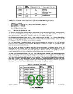
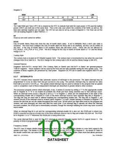
Register D
MSB
b7
LSB
b6
0
b5
b4
b3
b2
b1
B0
VRT
Day of month
VRT
The Valid RAM and Time (VRT) bit is cleared by the RTC to indicate that both the main power (VTR) and the battery
power (VBAT) are both low at the same time. This is the only case where the contents of the RAM, as well as, the
time and calendar registers are not valid. The VRT bit can only be set by a read of Register D. The Host can set the
VRT bit reading Register D after PWRGD =1.
b6
Read as zero and cannot be written.
b5:b0
Day of month Alarm; these bits store the day of month alarm value. If set to 000000b, then a don’t care state is
assumed. The host must configure the Day of month alarm for these bits to do anything, yet they can be written at
any time. If the Day of month alarm is not enabled, these bits will return zeros. These bits are not affected by
PCI_RESET, VTR_POR or VCC_POR. The BCD Range for the Day of month of month alarm is 1-31 and the Binary
Range is 01-1F.
Century Byte
The century byte is located at RTC/Bank0 register 0x32. The century byte is incremented by one when the year byte
changes from 99 or 0x63 to 0. The BCD Range for the century byte is 00-39 and the Binary Range is 00h-3Fh.
General Purpose
Registers 0xEh-0x7FH, except 0x32 (The Century Byte) in Bank0 and 0x0-0x7F in Bank1 are general-purpose
"CMOS" registers. These registers can be used by the host and are fully available during the time update cycle. The
contents of these registers are preserved by Vbat power. Registers Eh-7Fh are in bank0 and registers 80h-FFh are
in bank1.
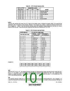
6.9.7 INTERRUPTS
The RTC includes three separate fully automatic sources of interrupts to the processor. The alarm interrupt may be
programmed to occur at rates from one-per-second to one-a-day. The periodic interrupt may be selected for rates
from half-a-second to 122.070 μs. The update-ended interrupt may be used to indicate to the program that an update
cycle is completed. Each of these independent interrupts are described in greater detail in other sections.
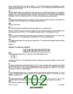
The processor program selects which interrupts, if any, it wishes to receive by writing a "1" to the appropriate enable
bits in Register B. A "0" in an enable bit prohibits the IRQB port from being asserted due to that interrupt cause.
When an interrupt event occurs a flag bit is set to a "1" in Register C, which are set independent of the state of the
corresponding enable bits in Register B. Each of the three interrupt sources have separate flag bits in Register C.
The flag bits may be used with or without enabling the corresponding enable bits. The flag bits in Register C are
cleared (record of the interrupt event is erased) when Register C is read. Double latching is included in Register C to
ensure the bits that are set are stable throughout the read cycle. All bits which are high when read by the program are
cleared, and new interrupts are held until after the read cycle. If an interrupt flag is already set when the interrupt
becomes enabled, the IRQB port is immediately activated, though the interrupt initiating the event may have occurred
much earlier.
When an interrupt flag bit is set and the corresponding interrupt-enable bit is also set, the IRQB port is driven low.
IRQB is asserted as long as at least one of the three interrupt sources has its flag and enable bits both set. The IRQF
bit in Register C is a "1" whenever the IRQB port is being driven low.
The serial interrupt that is used for the RTC interrupt is selected through register 0x70 of Logical Device 6. The
polarity of IRQ8 is programmable via bit 0 of register 0xF1 in Logical Device A.
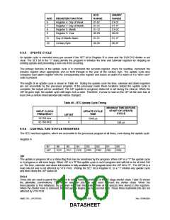
Frequency Divider
The RTC has 22 binary divider stages following the clock input. The output of the divider is a one Hertz signal to the
update-cycle logic. The divider is controlled by the three divider bits (DV2-DV0) in Register A. As shown in Table 50
the divider control bits can select the operating mode, or be used to hold the divider chain reset that allows precision
SMSC DS – LPC47S45x
Page 103 of 259
Rev. 07/09/2001
DATASHEET

 SMSC [ SMSC CORPORATION ]