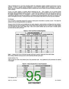
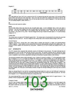
BASE
OFFSET
BANK
REGISTER TYPE
REGISTER FUNCTION
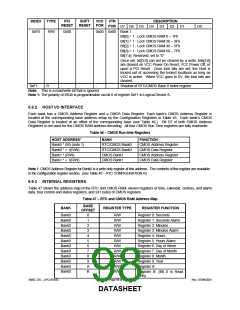
Bank0
Bank0
C
D
R
Register C:
R/W
Register D:
Day of Month Alarm
Century Byte
Bank0
Bank0
32
R/W
R/W
E-31,
33-7F
General purpose
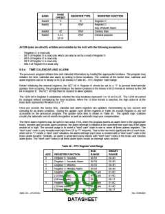
All 256 bytes are directly writable and readable by the host with the following exceptions:
-
-
-
-
-
Registers C is read only
Bit 7 of Register D is read only which can only be set by a read of Register D.
Bit 6 of Register D is read only .
Bit 7 of Register A is read only
Bits 0 of Register B is read only
6.9.4 TIME CALENDAR AND ALARM
The processor program obtains time and calendar information by reading the appropriate locations. The program may
initialize the time, calendar and alarm by writing to these locations. The contents of the twelve time, calendar and
alarm registers can be in binary or BCD as shown in Table 48 − RTC Register Valid Range.
Before initializing the internal registers, the SET bit in Register B should be set to a "1" to prevent time/calendar
updates from occurring. The program initializes the twelve locations in the binary or BCD format as defined by the DM
bit in Register B. The SET bit may then be cleared to allow updates.
The 12/24 bit in Register B establishes whether the hour locations represent 1 to 12 or 0 to 23. The 12/24 bit cannot
be changed without reinitializing the hour locations. When the 12 hour format is selected, the high order bit of the
hours byte represents PM when it is a "1".
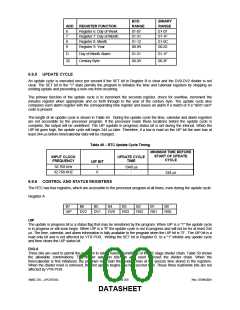
Once per second, the twelve time, calendar and alarm registers are updated, Incrementing by one second and
checking for an alarm condition. During the update cycle all the registers in Table 48, except Register D, are not
accessible by the processor program. The update cycle time is shown in Table 49. The update logic contains
circuitry for automatic end-of-month recognition as well as automatic leap year compensation.
The three alarm registers may be used in two ways. First, when the program inserts an alarm time in the appropriate
hours, minutes and seconds alarm locations, the alarm interrupt is initiated at the specified time each day if the alarm
enable bit is high. The second usage is to insert a "don't care” state in one or more of three alarms registers. The
"don't care" code is any hexadecimal byte from C0 to FF inclusive. That is the two most significant bits of each byte,
when set to "1" create a "don't care" situation. An alarm interrupt each hour is created with a "don't care" code in the
hours alarm location. Similarly, an alarm is generated every minute with "don't care" codes in the hours and minutes
alarm bytes. The "don't care" codes in all three alarm bytes create an interrupt every second.
Table 48 − RTC Register Valid Range
BCD
RANGE
00-59
BINARY
RANGE
00-3B
00-3B
00-3B
00-3B
01-0C
81-8C
00-17
ADD
REGISTER FUNCTION
Register 0: Seconds
Register 1: Seconds Alarm
Register 2: Minutes
Register 3: Minutes Alarm
Register 4: Hours
0
1
2
3
4
00-59
00-59
00-59
01-12 am
81-92 pm
00-23
(12 hour mode)
(24 hour mode)
5
Register 5: Hours Alarm
(12 hour mode)
01-12 am
81-92 pm
00-23
01-0C
81-8C
00-17
(24 hour mode)
SMSC DS – LPC47S45x
Page 99 of 259
Rev. 07/09/2001
DATASHEET

 SMSC [ SMSC CORPORATION ]