Note 2. This is Fan Control Register Bit 2 or 3
Note 3. This is Fan Control Register Bit 0 or 1
Note 4. This is FANx Register Bit 7
FANx Registers
The FAN1 and FAN2 Registers are located at 0x56 and 0x57 from base I/O in Logical Device A. The bits are defined
below. See the register description in the Runtime Registers section.
Fan x Clock Select Bit, D7
The Fan x Clock Select bit in the FANx registers is used with the Fan x Clock Source Select and the Fan x Clock
Multiplier bits in the Fan Control register to determine the fan speed FOUT. See Table 58 above.
Duty Cycle Control for Fan x, Bits D6 – D1
The Duty Cycle Control (DCC) bits determine the fan duty cycle. The LPC47M10x has ≈1.56% duty cycle resolution.
When DCC = “000000” (min. value), FOUT is always low. When DCC is “111111” (max. value), FOUT is almost always
high; i.e., high for 63/64th and low for 1/64th of the FOUT period.
Generally, the FOUT duty cycle (%) is (DCC ÷ 64) × 100.
Fan x Clock Control, Bit D0
The Fan x Clock Control bit D0 is used to override the Duty Cycle Control for Fan x bits and force FOUT always high.
When D0 = “0”, the DCC bits determine the FOUT duty cycle. When D0 = 1, FOUT is always high, regardless of the
state of the DCC bits.
Fan Control Register
The Fan Control Register is located at 0x58 from base I/O in Logical Device A. The bits are defined below. See the
register description in the Runtime Registers section.
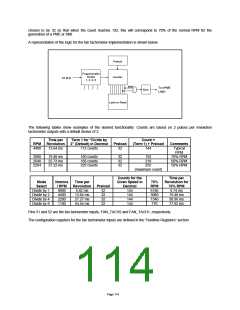
Fan x Count Divisor, Bits D7-D6 / D5-D4
Fan x Count Divisor bit in Fan Control Register is used to determine fan tachometer count. The choices for the
divisor are 1, 2, 4 and 8. See “Fan Tachometer Input” section.
Fan x Clock Multiplier, Bits D3 / D2
The Fan x Clock Multiplier bit is used with the Fan x Clock Source Select bit in the Fan Control Register and the Fan
x Clock Select bit in Fan register to determine the FOUT
.
When the Fan x Clock Multiplier bit = “0”, no clock multiplier is used. When the Fan x Clock Multiplier bit = “1”, the
clock speed determined by the Fan x Clock Source Select bit is doubled.
Fan x Clock Source Select, Bits D1 / D0
The Fan x Clock Source Select and the Fan x Clock Multiplier bits in the Fan Control register is used with The Fan x
Clock Select bit in the Fan x registers to determine the fan speed FOUT. See Table 58 above.
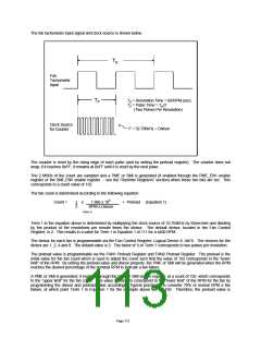
Fan Tachometer Inputs
The LPC47M10x implements fan tachometer inputs for signals from fans equipped with tachometer outputs. The part
can generate both a PME and an SMI when the fan speed drops below a predetermined value. See description
below.
The clock source for the tachometer count is the 32.768kHz oscillator. The Fan Tachometer Inputs gate a divided
down version of the 32.768kHz oscillator for one period of the Fan signal into an 8-bit counter (maximum count is
255).
The clock source is determined by the CLK32_PRSN bit in the CLOCKI32 register in logical device A. It is either the
32.768kHz clock from the CLKI32 pin or an internal 32.765kHz clock derived from the 14MHz clock.
Page 112

 SMSC [ SMSC CORPORATION ]