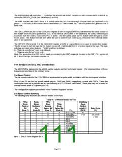
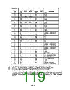
SECURITY FEATURE
The following register describes the functionality to support security in the LPC47M10x.
GPIO Device Disable Register Control
The GPIO pin GP43 is used for the Device Disable Register Control (DDRC) function. Setting bits[3:2] of the GP43
configuration register to ‘01’, selects the DDRC function for the GP43 pin. When bits[3:2]=01 the GP43 pin is an
input, with non-inverted polarity. Bits[3:2] cannot be cleared by writing to these bits; they are cleared by VTR POR,
VCC POR and Hard Reset. That is, when the DDRC function is selected for this pin, it cannot be changed, except by a
VCC POR, hard reset or VTR POR.
When the DDRC function is selected for GP43, the Device Disable register is controlled by the value of the GP43 pin
as follows:
•
•
If the GP43 pin is high, the Device Disable Register is Read-Only.
If the GP43 pin is low, the Device Disable Register is Read/Write.
Device Disable Register
The Device Disable Register is located in the PME register block at offset 0x22 from the PME_BLK base I/O address
in logical device A. Writes to this register are blocked when the GP43 pin is configured for the Device Disable
Register Control function (GP43 configuration register bit 2 =1) and the GP43 pin is high.
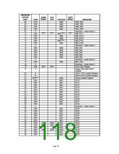
The configuration register for the device disable register is defined in the “Runtime Registers” section.
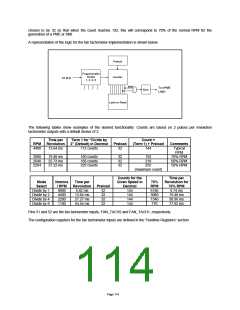
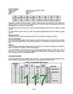
GAME PORT LOGIC
The LPC47M10x implements logic to support a dual game port. This logic includes the following for each game port:
two 555 timers, two game port RC constant inputs (x-axis and y-axis), two game port button inputs and game port
interface logic. The implementation of the Game Port uses a simple A/D converter constructed from a 555 timer to
digitize the analog value of a potentiometer for the x-axis and y-axis of the joystick.
The figure below illustrates the implementation of the game port logic in the LPC47M10x.
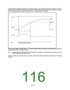
Game software will write a byte to the game port to reset it, and then poll (read) the port until the x and y-axis RC time
constant pins (TIMA,B) time out (return to zero). The elapsed time indicates the resistance value of the potentiometer
and in turn, the position of the joystick.
Internal To Joysticks
Internal To LPC47M10x
Vcc = 5V
556
J1X
J1Y
X-Axis
Y-Axis
Joystick 1
Vcc = 5V
TIM1A
OUT1A
OUT1B
TIM1B
JOYW
TRIG1A
TRIG1B
D0
D1
D2
D3
Vcc = 5V
Joystick 2
556
J2X
J2Y
X-Axis
TIM2A
OUT2A
OUT2B
Vcc = 5V
Y-Axis
JOYR
Game Port
Register
TIM2B
Vcc = 5V
TRIG2A
TRIG2B
J1B1
J1B2
J2B1
J2B2
Joystick 1 Button 1
Joystick 1 Button 2
D4
D5
D6
D7
Joystick 2 Button 1
Joystick 2 Button 2
Page 115

 SMSC [ SMSC CORPORATION ]