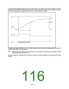
The figure below illustrates the timing of the game port signals. The 556 timers will reset the outputs (OUTA,B) to
zero and the RC constant (TIMA,B) pins to zero when the RC constant (TIMA,B) inputs reach 2/3 of VREF as shown.
VREF is the voltage on pin 44, which is either 5V or 3.3V. See the “VREF Pin “ section.
JOYW
VREF
2
3
VREF
TIMA,B
t1
OUTA,B
JOYR
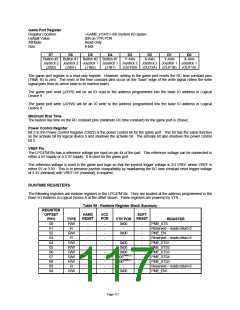
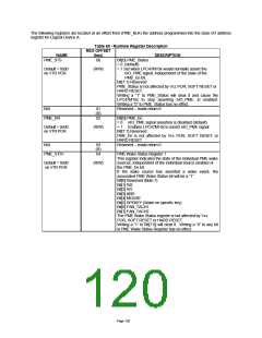
The game port register is defined below. It is a runtime register located at the address programmed into the base I/O
address (GAME_PORT) in Logical Device 9.
Note:
Register 0x60 is the high byte; 0x61 is the low byte. For example, to set the primary base address to 1234h,
write 12h into 0x60, and 34h into 0x61.
When the activate bit in Logical Device 9 is cleared, it prevents the base I/O address for the game port from being
decoded.
Page 116

 SMSC [ SMSC CORPORATION ]