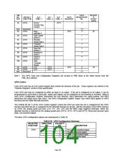
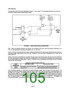
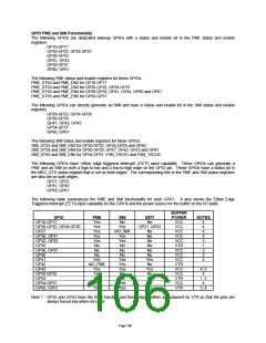
SYSTEM MANAGEMENT INTERRUPT (SMI)
The LPC47M10x implements a “group” nIO_SMI output pin. The System Management Interrupt is a non-maskable
interrupt with the highest priority level used for OS transparent power management. The nIO_SMI group interrupt
output consists of the enabled interrupts from each of the functional blocks in the chip and many of the GPIOs and
the Fan tachometer pins. The GP27/nIO_SMI pin, when selected for the nIO_SMI function, can be programmed to be
active high or active low via the polarity bit in the GP27 register. The output buffer type of the pin can be
programmed to be open-drain or push-pull via bit 7 of the GP27 register. The nIO_SMI pin function defaults to active
low, open-drain output.
The interrupts are enabled onto the group nSMI output via the SMI Enable Registers 1 to 5. The nSMI output is then
enabled onto the group nIO_SMI output pin via bit[7] in the SMI Enable Register 2. The SMI output can also be
enabled onto the serial IRQ stream (IRQ2) via Bit[6] in the SMI Enable Register 2. The internal SMI can also be
enabled onto the nIO_PME pin. Bit[5] of the SMI Enable Register 2 is used to enable the SMI output onto the
nIO_PME pin (GP42). This bit will enable the internal SMI output into the PME logic through the DEVINT_STS bit in
PME_STS3. See PME section for more details.
An example logic equation for the nSMI output for SMI registers 1 and 2 is as follows:
nSMI = (EN_PINT and IRQ_PINT) or (EN_U2INT and IRQ_U2INT) or (EN_U1INT and IRQ_U1INT) or (EN_FINT and
IRQ_FINT) or (EN_MINT and IRQ_MINT) or (EN_KINT and IRQ_KINT) or (EN_IRINT and IRQ_IRINT)
SMI Registers
The SMI event bits for the GPIOs and the Fan tachometer events are located in the SMI status and Enable registers
3-5. The polarity of the edge used to set the status bit and generate an SMI is controlled by the polarity bit of the
control registers. For non-inverted polarity (default) the status bit is set on the low-to-high edge. If the EETI function
is selected for a GPIO then both a high-to-low and a low-to-high edge will set the corresponding SMI status bit.
Status bits for the GPIOs are cleared on a write of ‘1’.
The P12 function also has a polarity select bit in Configuration Register 0xF0 in Logical Device 1.
The SMI logic for these events is implemented such that the output of the status bit for each event is combined with
the corresponding enable bit in order to generate an SMI.
The SMI registers are accessed at an offset from PME_BLK (see Runtime register section for more information).
The SMI event bits for the super I/O devices are located in the SMI status and enable register 1 and 2. All of these
status bits are cleared at the source except for IRINT, which is cleared by a read of the SMI_STS2 register; these
status bits are not cleared by a write of ‘1’. The SMI logic for these events is implemented such that each event is
directly combined with the corresponding enable bit in order to generate an SMI.
See the “Runtime Registers” section for the definition of these registers.
Page 108

 SMSC [ SMSC CORPORATION ]