The state machine will reset after 11 clocks and the process will restart. The process will continue until it is shut off by
setting the SPEKEY_EN bit (see following sub-section).
The state machine will reset if there is a period where the clock remains high for more than one keyboard clock
period (115-145usec) in the middle of the transmission (i.e., before clock 11). This is to prevent the generation of a
false PME.
The CLK32_PRSN bit (bit 0 of the CLOCKI32 register at 0xF0 in Logical Device A) will determine the clock source for
this feature when the part is powered by VCC. If the external 32kHz clock is not connected, the 32kHz internal signal
is derived from the 14MHz clock when VCC is active. Use the 32kHz clock for this feature when the part is under
trickle power. This feature will not work when the part is under trickle power (VCC removed) if the external 32kHz
clock is not connected.
The SPEKEY_EN bit at bit 1 of the CLOCKI32 register at 0xF0 in Logical Device A is used to control this feature.
This bit is used to turn the logic for this feature on and off. It will disable the 32 kHz clock input to the logic. The logic
will draw no power when disabled. The bit is defined as follows:
0= “Wake on specific key” logic is on (default)
1= “Wake on specific key” logic is off
Note: The generation of a PME for this event is controlled by the PME enable bit (located in the PME_EN1 register at
bit 5) when the logic for feature is turned on.
FAN SPEED CONTROL AND MONITORING
The LPC47M10x implements fan speed control outputs and fan tachometer inputs. The implementation of these
features are described in the sections below.
Fan Speed Control
The fan speed control for the LPC47M10x is implemented as pulse width modulators with fan clock speed selection.
Pins 54 and 55 are the fan speed control outputs, FAN2 and FAN1, respectively, muxed with GPIOs. These fan
control pins come up as outputs and are low following a VCC POR and Hard Reset. These pins may not be used for
wakeup events under VTR power (VCC=0).
The configuration registers are defined in the “Runtime Registers” section.
Fan Speed Control Summary
The following table illustrates the different modes for the fans.
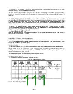
Table 58 – Different Modes for Fan
FANx
Clock
Control
Bit
(Note 1)
FANx
Clock
Multiplier
Bit
(Note 2)
FANx
Clock
Source
Select Bit
(Note 3)
X
6-Bit Duty
Cycle
Control
bits[6:1]
(DCC)
0
FANx
Clock
Select Bit
(Note 4)
Duty Cycle
Fout
0Hz – LOW
15.625kHz
23.438kHz
40Hz
(%)
-
(DCC/64)
• 100
0
0
0
0
0
0
0
0
0
1
X
0
0
0
0
1
1
1
1
X
X
0
1
0
1
0
1
0
1
X
0
0
1-63
1
1
0
0
1
1
X
60Hz
31.25kHz
46.876kHz
80Hz
120Hz
0Hz – HIGH
-
-
Note 1. This is FANx Register Bit 0
Page 111

 SMSC [ SMSC CORPORATION ]