1=The group SMI output is active.
Note: Bit 5 of the SMI_EN2 register must also be set.
This bit is cleared on a write of ‘1’.
There is a bit in the PME Enable Register 3 to enable the SMI onto the nIO_PME pin (if the nIO_PME function is
selected for GP42). This bit, DEVINT_EN, is at bit 3 of the PME_EN3 register. This bit will enable the internal “group”
SMI signal (if bit 5 of the SMI_EN2 register is set) into the PME logic through the DEVINT_STS bit as follows: If the
DEVINT_EN bit is ‘1’ and the DEVINT_STS bit is ‘1’ then the nIO_PME pin will be active. This pin has its polarity
controlled by the polarity bit in the GP42 register.
This bit is defined as follows:
0=Disable group SMI output from the nIO_PME pin.
1=Enable group SMI output onto the nIO_PME pin. That is, if this bit is set and the DEVINT_STS bit is set then a
nPME is generated.
Note: Bit 5 of the SMI_EN2 register must also be set.
‘WAKE ON SPECIFIC KEY’ OPTION
The LPC47M10x has logic to detect a single keyboard scan code for wakeup (PME generation). The scan code is
programmed onto the Keyboard Scan Code Register, a runtime register at offset 0x5F from the base address located
in the primary base I/O address in Logical Device A. This register is powered by VTR and reset on VTR POR.
The PME status bit for this event is located in the PME_STS1 register at bit 5 and the PME enable bit for this event is
located in the PME_EN1 register at bit 5. See the Runtime Register section for a definition of these registers.
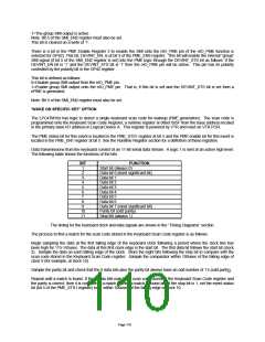
Data transmissions from the keyboard consist of an 11-bit serial data stream. A logic 1 is sent at an active high level.
The following table shows the functions of the bits.
BIT
1
FUNCTION
Start bit (always 0)
2
3
Data bit 0 (least significant bit)
Data bit 1
4
Data bit 2
5
Data bit 3
6
Data bit 4
7
Data bit 5
8
Data bit 6
9
10
11
Data bit 7 (most significant bit)
Parity bit (odd parity)
Stop Bit (always 1)
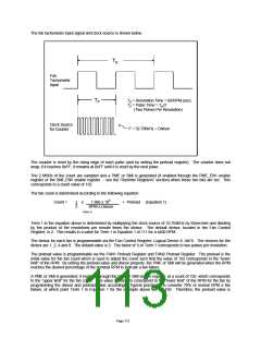
The timing for the keyboard clock and data signals are shown in the “Timing Diagrams” section.
The process to find a match for the scan code stored in the Keyboard Scan Code register is as follows:
Begin sampling the data at the first falling edge of the keyboard clock following a period where the clock line has
been high for 115-145usec. The data at this first clock edge is the start bit. The first data bit follows the start bit (clock
2). Sample the data on each falling edge of the clock. Store the eight bits following the stop bit to compare with the
scan code stored in the Keyboard Scan Code register. Sample the comparator within 100usec of the falling edge of
clock 9 (for example, at clock 10).
Sample the parity bit and check that the 8 data bits plus the parity bit always have an odd number of 1’s (odd parity).
Repeat until a match is found. If the 8 data bits match the scan code stored in the Keyboard Scan Code register and
the parity is correct, then it is considered a match. When a match is found and if the stop bit is 1, set the event status
bit (bit 5 of the PME_STS1 register) to ‘1’ within 100usec of the falling edge of clock 10.
Page 110

 SMSC [ SMSC CORPORATION ]