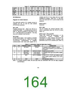
Table 71 - ACCESS.BUS Control/Status Register S1
Control
R/W
D7
W
D6
W
D5
W
D4
W
D3
W
D2
W
D1
W
D0
W
Bit Def
PIN
ES0
Reserved
Reserved
ENI
STA
STO
ACK
Status
R/W
D7
R
D6
R
D5
R
D4
R
D3
R
D2
R
D1
R
D0
R
Bit Def
PIN
0
STS
BER
LRB
AAS
LAB
nBB
enabled and the S1 bus status bits are made
available for reading. With ESO = 0, bits ENI,
STA, STO and ACK of S1 can be read for test
purposes.
Bit Definitions
Register S1 Control Section
The write-only section of S1 enables access to
registers S0, S0’, S1 and S2, and controls
ACCESS.bus operation.
BITS 5 and 4
Reserved.
BIT 3: ENI
BIT 7 PIN
This bit enables the internal interrupt, nINT,
which is generated when the PIN bit is active
(logic “0”).
Pending Interrupt Not. When the PIN bit is
written with a logic “1”, all status bits are reset to
logic “0”, with the exception of PIN which is set
to “1”, and nBB which is not affected. This may
serve as a software reset function.
BITS 2 and 1, STA and STO
These bits control the generation of the
ACCESS.bus
START
condition
and
BIT 6 ESO
transmission of slave address and R/nW bit,
generation of repeated START condition, and
generation of the STOP condition (see Table 72)
Enable Serial Output. ESO enables or disables
the serial ACCESS.bus I/O. When ESO is high,
ACCESS.bus communication is enabled;
communication with serial shift register S0 is
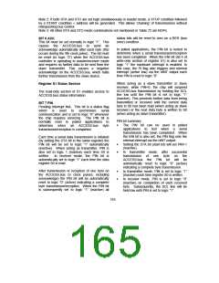
Table 72 - Instruction Table for Serial Bus Control
STA
1
STO
0
PRESENT MODE
FUNCTION
START
OPERATION
Transmit START+address, remain
MST/TRM if R/nW#=0; go to MST/REC
if R/nW=1.
SLV/REC
1
0
0
1
MST/TRM
MST/REC;
MST/TRM
MST
REPEAT START
STOP READ;
STOP WRITE
Same as for SLV/REC
Transmit STOP go to SLV/REC mode;
Note 1
Send STOP, START and address after
last master frame without STOP sent;
Note 2
1
1
DATA CHAINING
0
0
ANY
NOP
No operation; Note 3
Note 1: In master receiver mode, the last byte must be terminated with ACK bit high (‘negative
acknowledge’)
164

 SMSC [ SMSC CORPORATION ]