ACCESS.bus
The FDC37C93xFR supports ACCESS.bus.
device driver interface, and several specific
device protocols.
ACCESS.bus is a serial communication protocol
between a computer host and its peripheral
devices. It provides a simple, uniform and
inexpensive way to connect peripheral devices
to a single computer port. A single ACCESS.bus
For a description of the ACCESS.bus protocol,
please refer to the ACCESS.bus Specifications
Version 2.2, February 1994, available from the
ACCESS.bus Industry Group.
on
a host can accommodate up to 125
peripheral devices.
The ACCESS.bus interface is based on the
PDC8584 controller. The registers are mapped
into the ISA I/O register space as set by the
configuration registers. The addresses for the
registers are shown in Table 70.
The ACCESS.bus protocol includes a physical
layer based on the I2C serial bus developed by
Philips, and several software layers.
The
software layers include the base protocol, the
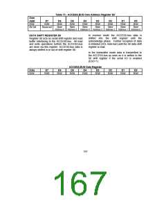
Table 70 - ACCESS.bus Register Addresses
Address (Note 1)
Base+0
Base+1
Register
Control/Status
Own Address
Data
Base+2
Base+3
Clock
Note 1: Base I/O Range: [0x00:0x0FFC] ON 4 BYTE BOUNDARIES
ACCESS.bus status information required for bus
REGISTERS
access and or monitoring.
The ACCESS.bus interface has four internal
register locations. Two of these, own address
register S0’ and clock register S2, are used for
initialization of the chip. Normally they are only
written once directly after resetting of the chip.
The other two registers, the data shift register
S0, and the control/status register S1, (which
functions as a double register) are used during
actual data transmission/reception. Register S0
performs all serial-to-parallel interfacing with the
ACCESS.Bus Control/Status Register S1
The control/status register controls the
ACCESS.bus operation and provides status
information. This register has separate read and
write functions for all bit positions. The write-
only section provides register access control
and control over ACCESS.bus signals, while the
read-only section provides ACCESS.bus status
information.
ACCESS.bus.
Register
S1
contains
163

 SMSC [ SMSC CORPORATION ]